Introduction
At high frequencies, the conductor and dielectric losses lead to dispersion of the transmitted signal. The total loss of the transmission path is the sum of dielectric and conductor losses. Predicting total loss using smooth copper and published loss tangent values is no longer adequate in the 10-plus GB/s regime.
Conductor loss is due to the redistribution of current, caused by skin-effect, and increases in proportion to the square-root of frequency. Total conductor loss is the sum of the actual conductor and return path losses. Surface roughness further exacerbates both due to increased surface area caused by the tooth structure.
The traditional Hammerstad-Jensen model has been used for decades to account for increased losses. This model is based solely on a mathematical fit to power loss data published by S.P. Morgan in 1949. There is no theoretical basis to support it and has bandwidth limitations.
The more recent Huray model is based on a collection of spheres, resembling “snowballs”, stacked in a pyramid geometry. If the size and number of spheres are known, a roughness correction factor can be analytically solved through a simple equation. The problem has always been getting the necessary parameters from sophisticated Scanning Electronic Measurements (SEM) and fitting them with empirical data through simulation.
In a DesignCon 2013 paper [5], the authors compare both models. They discuss why it is often impractical to use information directly from manufacturers’ data sheets because they are not always in a format that immediately translates into mathematical parameters for commercial simulators. Instead, they rely on empirical data from a test board to fit parameters associated with conductor and dielectric losses. Later they use these parameters in circuit simulators to create scalable transmission line models for any interconnect of similar construction.
The motivation of this research work was to develop a practical method for modeling surface roughness from first principles alone. By accepting roughness parameters solely from manufacturers’ data sheets, we show how to determine the sphere radius and tile area parameters used in the Huray model. Using a close packing of equal spheres model, conductor loss can now be accurately predicted without the need of additional SEM data, or test board fitted parameters.
We show that when measurements from Megtron6 and N4000-13EP test boards were compared to simulations using this model, there was excellent correlation to 25 GHz.
Background
The total loss of a printed circuit board (PCB) transmission line, as a function of frequency, is the sum of dielectric and conductor loss as shown by example in Figure 1. The difference between the simulated total loss and measured loss is due to conductor surface roughness.
In this example, the foil type used was very low profile (VLP). Although it is a relatively smooth foil, compared to the standard foil, failure to model roughness effects for designs running at 25GB/s can ruin you day.

Figure 1. Comparisons of measured insertion loss vs simulated conductor, dielectric and total insertion loss of conductor. Modeled and simulated with Keysight EEsof EDA ADS software [21].
Figure 2 shows eye diagrams at 25 Gb/s for measured loss with rough copper (left) and total loss of smooth copper (right). With just -3.5dB delta in insertion loss at 12.5 GHz, there is half the eye height opening with rough copper.


Figure 2. Simulated eyes of measured loss with rough copper (left) vs smooth copper (right) at 25 Gb/s. Modeled and simulated with Keysight EEsof EDA ADS software [21].
Conductor Loss Model
The distribution of current propagating through a rectangular conductor at DC is uniform. The resistance per unit length is proportional to the bulk resistivity of the conductor’s material and inversely proportional to the cross sectional area [1]:
Equation 1

Where: RDC_cond = DC resistance per meter in ohms/meter; ρ = bulk resistivity of the material. For annealed copper ρ = 1.72E-8 ohm-meters; w = conductor width in meters;t = conductor thickness in meters.
For AC, the conductor loss increases in proportion to the square-root of frequency. This is due to the redistribution of current towards the outer edges caused by skin-effect. The resulting skin-depth (δ) is the effective thickness where the current flows around the perimeter and is a function of frequency. As frequency increases, skin depth decreases, thereby increasing the AC resistance.


Figure 3. DC current distribution through a rectangular conductor (left) and AC current distribution (right). Skin-depth (δ) is the effective thickness where the current flows and is a function of frequency
Skin-depth at a particular frequency is determined by [1]:
Equation 2

Where: δ = skin-depth in meters; f = sine-wave frequency in Hz; μ0= permeability of free space =1.256E-6 Wb/A-m; σ = conductivity in S/m. For annealed copper
σ = 5.80E7 S/m.
When the skin depth is smaller than the thickness, the resistive loss per unit length of the conductor can be approximated by:
Equation 3

The distributed resistance of a transmission line includes the resistance of the signal conductor plus the resistance of the return conductor or reference plane(s). In microstrip, the high frequency currents through the signal conductor are concentrated mostly along the surface facing the reference plane, as shown in Figure 4. The return current distribution density in the reference plane is spread out to roughly +/-3H from the signal conductor’s center, with the highest concentration near the center [6].


Figure 4. High frequency current density distribution of microstrip (left) and stripline (right) when the skin depth is much less than the thickness of the conductor.
In stripline, the high frequency currents are concentrated primarily along the top and bottom surfaces of the signal conductor. The current density is dependent on the signal conductor’s proximity to the upper and lower reference planes. If H1 = H2, then the current divides equally along the top and bottom surfaces of the signal conductor. The return current distribution on the respective reference planes are spread out +/-3H1 and +/-3H2 from the signal conductor’s center. If H1 = H2, then the current distribution density is the same through both reference planes.
In an offset stripline (not shown), the signal conductor is skewed closer to one reference plane and therefore, the current density will be higher along the respective surfaces closest to each other.
The AC resistance per unit length of a microstrip can be approximated by [6]:
Equation 4

Where:
w = width of the conductor in meters;t = conductor thickness in meters;H = height of conductor to reference plane in meters;ρ = bulk resistivity of copper =1.72E-8 ohm-meters; μ0 = permeability of free space = 1.256E-6 Wb/A-m.
The AC resistance per unit length of a stripline, or offset stripline, can be approximated by first determining the AC resistance of top and bottom surface of the signal conductor separately using Equation 4; then combine the two in parallel. Hence, the total AC resistance (RAC_stripline) is determined by [6]:
Equation 5

Where:

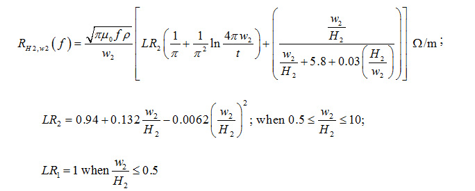
w1, w2 are the widths at the bottom and top of a conductor in meters respectively;
t = conductor thickness in meters; H1 is height to bottom reference plane in meters; H2 is height to top reference plane in meters;ρ = the bulk resistivity of copper = 1.72E-8 ohm-meters; μ0 = permeability of free space = 1.256E-6 Wb/A-m.
The insertion loss of a smooth rectangular stripline conductor, as a function of frequency, is determined by:
Equation 6

Where:ILsmooth (f) = insertion loss of a smooth conductor, as a function of frequency, in dB/meter; αsmooth (f) = attenuation constant of a smooth conductor, as a function of frequency, in dB/meter;RAC_stripline (f)= AC resistance of a smooth conductor, as a function of frequency, in ohms/meter;Zo (f) = characteristic impedance of the transmission line, as a function of frequency, in ohms;e = base of natural logarithm.
Conductor Loss Model Validation
Keysight EEsof EDA Momentum 3D Planar EM Simulator [21]was used to validate the conductor loss model. A 4 inch stripline model was constructed with dielectric and copper parameters shown in Figure 5. To isolate conductor loss from the total loss, the dissipation factor (Df) of the dielectric was set to zero. The conductivity of annealed copper was set to 5.8 S/m for both conductor and reference planes.


Figure 5. Keysight EEsof Momentum [21]substrate parameters for a 4 inch stripline copper trace. Lossless dielectric parameters used to isolate conductor loss during simulation.
Figure 6 compares the simulation results of the loss model versus the 3D simulation. Remarkably there is excellent correlation to validate the model.
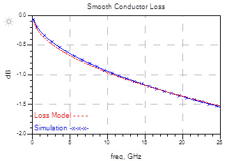
Figure 6. Simulation results comparing Momentum 3D planar stripline model with conductor loss model.
Loss Due to Copper Roughness
In PCB construction there is no such thing as a perfectly smooth conductor surface. Some degree of roughness is always applied to promote adhesion to the dielectric material. Unfortunately, increasing copper roughness contributes to additional conductor loss.
Rolled and electro-deposited (ED) are two copper foil fabrication processes used in PCB laminate construction today. Of the two, rolled copper will always be smoother than standard ED copper.
Rolled copper foil starts with a billet of pure copper fed into a series of progressively smaller rollers to achieve the final thickness. The smoothness of the rollers ultimately determines the final smoothness of the foil.
The ED copper process sees a large rotating drum, made of polished stainless steel or titanium, which is partially submerged in a bath of copper sulfate solution. The cathode terminal is attached to the drum, while the anode terminal is submerged in the solution. A DC voltage supplies the anode and cathode with the correct polarity.
As the drum slowly rotates, copper is deposited onto it. The final thickness is inversely proportional to the drum speed. I.E., the faster the drum rotation, the thinner the copper foil.
A finished sheet of ED copper foil has two sides. The matte side faces the copper sulfate bath, while the drum side faces the rotating drum. Consequently, the drum side is always smoother than the matte side.
After the foil is peeled away from the drum, the matte and drum side go through separate treatment cycles, in order to prepare it for the laminate fabrication process. The matte side is usually attached to the prepreg sheets, prior to final pressing and curing, to form the core laminate. To enhance adhesion, the matte side has additional treatment applied to roughen the surface.
For high frequency boards, sometimes the drum side of the foil is laminated to the prepreg. In this case it is referred to as reversed treated foil (RTF). Even after treatment, it is still smoother than standard treated foils.
Various foil manufacturers offer ED copper foils with varying degrees of roughness. The root-mean-square (RMS) height of these profiles can range from approximately 0.3 μm to 5.8 μm [6]. Each supplier tends to market their product with their own brand name. Presently, there seems to be three distinct classes of copper foil:
- Standard
- Very-low profile (VLP)
- Ultra-low profile (ULP) or profile free (PF).
Some other common names referring to ULP class are HVLP or eVLP.
An etch treatment is often used to roughen the surface of the drum side before lamination to improve dielectric adhesion. CO-BRA BOND® SM [20]is one example of a hydrogen peroxide/sulfuric acid micro-etch treatment used by PCB fabricators.
Modeling Copper Roughness
Several modeling methods were developed over the years to determine a roughness correction factor (Ksr). When multiplicatively applied to the smooth conductor attenuation (αsmooth), the attenuation due to roughness (αrough) can be determined by:
Equation 7

The most popular method has been the Hammerstad and Jensen (H&J) model, based on work done in 1949 by S. P. Morgan. Most recently, the Huray model [9]has gained popularity due to the continually increasing data rate’s need for better modeling accuracy.
Hammerstad and Jensen Model
The H&J model assumes a triangular corrugated surface, representing the tooth structure of rough copper, as shown in Figure 7. When the skin depth is small, compared to the tooth height, current begins to flow along the corrugated surface; thereby increasing its loss due to the longer path length. However, the theory breaks down from a physics perspective because there is no evidence of additional time delay (TD), compared to the fixed spatial length of the trace.


Figure 7. A two-dimensional surface profile the H&J model is based on.
The H&J correction factor (KHJ), at a particular frequency, is determined by:
Equation 8

Where: KHJ = H&J roughness correction factor;∆ = RMS tooth height in meters;
δ = skin depth in meters.
It is solely based on a mathematical fit to S. P. Morgan’s power loss data. There is no theoretical basis to support it.
The model has correlated well for microstrip geometries up to about 15 GHz, for surface roughness of less than 2  RMS. However, it proved less accurate for frequencies above about 5GHz for very rough copper [6].
A modified H&J empirical fit scaling factor term [5]is multiplicative to the basic H&J equation to account for increased surface area:
Equation 9

SF is the scaling factor representing the ratio of the length of the rough surface to the spatial length. When SF = 2, the equation reduces to the original H&J equation.
This model is impractical from a first principles perspective because SF is not normally published from foil manufactures. Instead, it can be used in conjunction with a “practical-feedback based design flow” method, as described in [5], to extract the relevant parameters from empirical measurements.
Huray Model
The Huray model, on the other hand, takes a real world physics approach to explain losses due to surface roughness. The model is based on a non-uniform distribution of spherical shapes resembling “snowballs” and stacked together forming a pyramidal geometry, as shown by the scanned electron microscope (SEM) photo [11]in Figure 8.
By applying electromagnetic wave analysis, the superposition of the sphere losses can be used to calculate the total loss of the structure. Since the losses are proportional to the surface area of the roughness profile, an accurate estimation of a roughness correction factor (KSRH) can be analytically solved by [5]:
Equation 10

Where: KSRH (f) = roughness correction factor, as a function of frequency, due to surface roughness based on the Huray model;  = relative area of the matte base compared to a flat surface; ai = radius of the copper sphere (snowball) of the ith size, in meters;
  = number of copper spheres of the ith size per unit flat area in sq. meters; δ (f) = skin-depth, as a function of frequency, in meters.
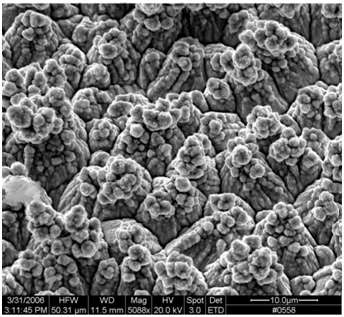

Figure 8. SEM photograph of electrodeposited copper nodules resembling “snowballs” on top of heat treated base foil. Photo courtesy [11].
It is theoretically possible to build an accurate snowball model of the surface roughness by extracting parameters through detailed analysis of SEM photographs. But practically, it is beyond the capabilities of most companies who do not have access to such equipment. Even if such equipment was available, the size, number of spheres and general tooth shape must be approximated anyways.
Early versions of the snowball model attempted to replicate real world roughness profiles by building facsimiles of low and high profile tooth structures, using a stack of uniform spheres, as shown in Figure 9. Each sphere had a radius of less than 1μm to fit a stack height of less than 5.8μm RMS because that was the dominant size of snowballs, as measured from SEM data, in either high or low profile examples [10]. A hexagonal tile base, with a width of 9.4μm RMS, was chosen to allow for replication into a lattice structure.
Eleven snowballs was the minimum number to fit within the hexagonal area and pyramid height of 5.8μm RMS. Thirty-eight was the maximum number. This modeling method did not attempt to optimize the size or number of snowballs in a pyramid, but instead was used to set limits for fitting to measured data.
This fitting method proved to be just as accurate as the modified H&J equation, as described earlier, but still relies on building a representative test coupon to extract parameters for detailed simulations. It is not any better for first principle analysis.
As a result, the motivation of this work was to develop an accurate method to model conductor losses due to surface roughness from first principles alone. This is desirable to perform what-if loss analysis at the front end of a design process, and help guide the final selection of board materials for preliminary PCB stackup design. It also helps gain intuition to sanitize further simulated results or analyze measured data.


Figure 9. Surface protrusions of a rough surface modeled by 11 spheres stacked within a hexagonal tile and replicated into a lattice structure [10].
Hexagonal Close-packing of Equal Spheres Model
Building upon the work already done by Huray et al [10], the concept of hexagonal close-packing of equal spheres (HCPES) is introduced to model the surface roughness (Patent pending). The difference between the HCPES model and the Huray stacked sphere approximation model is that the HCPES model determines the exact sphere diameter and hexagonal base area solely on roughness height published in manufacturers’ data sheets or measured by optical profilometers.
Recalling that losses are proportional to the surface area of the roughness profile, a simpler model can be used to optimally represent the surface roughness. Using the principle of HCPES [7], eleven uniform sized spheres, with radius (r), can be stacked on a hexagonal base, as illustrated in Figure 10.


Figure 10. HCPES model showing a stack of 11 uniform size spheres with radius r (left) and replicated into a lattice structure (right)
HCPES Correction Factor
Because the HCPES model assumes the nodule treatment is applied to a perfectly flat surface, the ratio of Amatte/Aflat = 1, and thus Equation 10 can be simplified to:

Equation 11
Where: KHCPES (f)= roughness correction factor, as a function of frequency, due to surface roughness based on the HCPES model;r = sphere radius in meters; δ (f) = skin-depth, as a function of frequency in meters; AHex = area of a single hexagonal tile base surrounding the seven base spheres in sq. meters.
Determining the RMS Height for HCPES Model
In lieu of SEM analysis, profilometers are often used to quantify the roughness tooth profile of electro-deposited copper. Figure 11shows schematically a profile of a rough conductor surface.
Tooth profiles are typically reported in terms of average roughness (Ra) for the drum side, and 10-point mean roughness (Rz) for the matte side. Most foil manufactures publish these parameters in their respective data sheets. Sometimes the RMS roughness (Rq) is also reported.
The average surface roughness parameter (Ra) is the arithmetic average of the absolute values of deviations Yi over the sample length.
The10-point height parameter (Rz), is the sum of the average of the five highest peaks (YP1, YP2 … YP5) and the five lowest valleys (YV1, YV2 … YV5), of the rough conductor surface over the sample length.


Figure 11. Schematic profile illustration of a rough conductor profile as measured with a profilometer
Figure 12 shows a cross-sectional view of a typical PCB conductor. The conductor has rough surfaces on a matte side (bottom) and a drum side (top). The matte side has a rougher surface than the drum side. Usually etching of the trace causes the conductor to have a trapezoidal shape.


Figure 12. Cross-sectional view of a rough conductor. The conductor has a rougher surface on a matte side (bottom) compared to the drum side (top).
For the purpose of determining the RMS height of the matte and drum sides of a rough conductor, a dual triangular sawtooth profile (DTSP) model is used, as illustrated in Figure 13(not to scale). The matte side is modeled by a matte triangular sawtooth profile (MTSP) with a peak-peak height RMTSP = Rz. The drum side is modeled by a drum triangular sawtooth profile (DTSP) with a peak-peak height RDTSP = Ra.


Figure 13. Dual triangular sawtooth profile (DTSP) model (not to scale) of the conductor profile used to determine HRMS of the matte and drum side.
The RMS height HRMSa, in meters, of the DTSP is approximated by Equation 12and the RMS height HRMSz, in meters, of the MTSP is approximated by Equation 13below:
Equation 12

Equation 13

An etch treatment may be applied to the drum side to facilitate adhesion to a substrate material. In that case, the average roughness (Ra) of the etch treatment is substituted for the drum side roughness when determining the respective RMS height.
Determining the HCPES Model Radius of Uniform Equal Spheres
Figure 14 shows an exploded view (top left), an isometric view (bottom left), top view (top right) and front view (bottom right) of the HCPES model. There are 11 equal spheres forming a pyramid-like shape on a hexagonal tile base. The model has 7 spheres in the bottom row, 3 spheres in the middle row and 1 sphere in the top row. The height of the pyramid-like shape is equal to the conductor surface roughness parameter HRMS. The hexagonal tile base completely surrounds the 7 spheres of the first row exactly.


Figure 14. HCPES model exploded view (top left) and isometric view (bottom left). Top right shows the top view and bottom right shows the front view of the model.
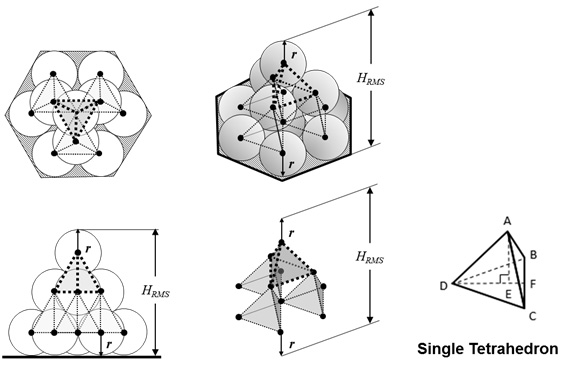

Figure 15. HCPES model with tetrahedron lattice structure. Three tetrahedrons form a stacked lattice structure connecting the centers of all 11 spheres. Total height (HRMS) equals the stacked height of 2 tetrahedrons (2AE) plus the diameter (2r) of a single sphere.
Figure 15 are orthographic and isometric views of the HCPES model. As shown, 3 tetrahedrons form a stacked lattice structure, connecting the centers of all 11 spheres. A single tetrahedron, labeled ABCD, is also shown for reference. Given that each side of the tetrahedron = 2r, the single tetrahedron height AE is determined as follows:

The total height HRMS is equal to the height of two tetrahedrons plus two radii of spheres:

And therefore the sphere radius (rHCPES), in meters, is determined by:
Equation 14

Determining the Area of the Hexagon Tile Base
The area of the hexagonal tile base can be determined with the aid of Figure 16


Figure 16. HCPES model used to determine area of hexagonal tile base.
Given:
ADG = Equilateral Triangle
ADF = 30:60:90 Triangle
BDE = 30:60:90 Triangle
BC = BE = r
DE = DF – r

If the area of the hexagon equals 6 times the area of triangle ADG, then the surface area of hexagon base AHex, in sq. meters, is determined by:
Equation 15

AC Resistance Due to Surface Roughness
To determine the AC resistance of a conductor, due to surface roughness, a single stripline is used as an example. Microstrip is not discussed since it is a subset of this method.
Figure 17 depicts a cross-sectional view of a single stripline. Typically the matte side of the signal conductor and the matte side of the reference plane are bonded to the core laminate. Similarly, the drum side of the signal conductor is bonded to the drum side of the adjacent reference plane with prepreg during final pressing of the entire PCB stackup. Before pressing the cores together, the drum side is roughened with an etch treatment to promote adhesion. This is usually the standard construction method. Sometimes, the drum side is treated then laminated to both sides of the core laminate instead. This process is known as drum side treated foil (DSTF) or reverse treated foil (RTF).


Figure 17. Cross-sectional view of a single stripline transmission line with surface roughness.
1. The AC resistance, as a function of frequency, for the matte and drum surfaces is determined as follows [6]:


2. Using the 10-point mean roughness parameter (Rz) for the matte side and average roughness parameters (Ra) for the drum surfaces (with etch treatment), the respective RMS heights, in meters, are approximately:

3. As a first approximation, it is assumed the matte surfaces of the conductor and reference plane have the same roughness value. Likewise for the drum surfaces. Therefore the correction coefficients for the matte and drum surfaces, based on the HCPES model described earlier, is determined by:
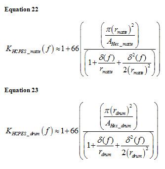
Where: KHCPES_matte (f) = matte surface correction coefficient as a function of frequency; KHCPES_drum (f) = drum surface correction coefficient as a function of frequency; = skin-depth as a function of frequency in meters.

4. The roughness correction coefficients are applied to the respective AC surface resistances, then combined in parallel to determine the final AC resistance of the stripline:

Case Study
To test the accuracy of the HCPES model, generalized modal S-parameters (GMS) reported in [5]and [12]were used in this case study. This data was courtesy of Molex Incorporated [17].
The same design was fabricated with both Panasonic’s Megtron-6 [18](with HVLP foil) and Nelco’s N4000-13EP [19](with VLP foil) material. Dielectric parameters for Dk and Df were obtained from the respective supplier’s published data sheets. Typical copper roughness data for HVLP and VLP foil data sheets were provided by respective laminate suppliers upon special request.
Two case studies were done for comparison. Case1 used Megtron-6 data and Case 2 used N4000-13EP data. The parameters are summarized in Table 1. Etch treatment was unknown so CO-BRA BOND® SM [20]was assumed.
For the N4000-13EP material, Dk was specified as 3.6-3.7 and Df at 0.008-0.009. For the simulation, the average was used for both parameters.
Table 1. Typical test board parameters obtained from manufacturers’ data sheets and design objective.
|
Parameter |
Case 1 Megtron-6 |
Case 2 N4000-13EP |
|---|---|---|
|
Dk |
3.62 @50GHz |
3.6-3.7 @10GHz[†] |
|
Df |
0.006 @ 50GHz |
0.008-0.009 @ 10GHz[‡] |
|
RzHVLP |
1.50 μm |
- |
|
RzVLP |
- |
2.50 μm |
|
Raw/Micro-etch[§] |
1.44 μm |
1.44 μm |
|
Trace Thickness, t |
15.23μm |
15.23μm |
|
Trace Widths w1, w2 |
251μm, 236 μm |
251μm, 236 μm |
|
Dielectric Heights, H1,H2 |
249μm, 231 μm |
249μm, 231 μm |
|
GMS trace length |
10.15 cm (4.00 in) |
10.15 cm (4.00 in) |
|
Zo(fo)ohms[**] |
52.29 @ 50GHz |
52.07 @ 10GHz |
[1] Dk= 3.65 used
[1] Df = 0.0085 used
[1] CO-BRA BOND® SM [20]is an example of a hydrogen peroxide/sulfuric acid micro-etch treatment often used by PCB fabricators to improve the adhesion of copper surface to dielectric materials.
[1]Zo(fo) = Characteristic impedance determined by 2D field solver at frequency fo
The total insertion loss (IL) is the sum of rough conductor and dielectric insertion losses:
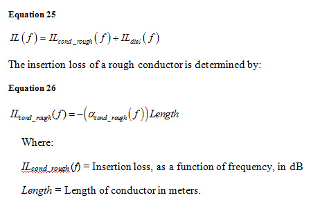
Where:
ILcond_rough (f)= Insertion loss, as a function of frequency, in dB
Length = Length of conductor in meters.

 To ensure causality, the model used to define Zo (f) is similar to the wideband Debye model to determine the relative dielectric constant Dk (f) described in [2].
Dielectric loss was modeled using Keysight EEsof EDA ADS software [21], per the general schematic shown in Figure 18. Causality was ensured by using the Svensson/Djordjevic wideband Debye model. By setting the conductivity parameter to a value much-much greater than the normal conductivity of copper ensures the conductor is lossless for the simulation.
Since there was no practical way to separately apply the respective HCPES correction coefficients to the matte and drum surfaces separately within ADS or Momentum, the smooth and rough conductor insertion losses were determined by equation functions within ADS, then added to the dielectric insertion loss output in the final plot after simulation.

Figure 18. Generic schematic used to simulate dielectric loss over frequency and Touchstone S-parameter measured data. Modeled with Keysight EEsof EDA ADS software [21]
Summary and Results
The results of analysis for Case 1 and Case 2 are plotted in Figure 19 and Figure 20, respectively. The insertion losses for smooth copper are also plotted for comparison.
Remarkably there is excellent agreement by just using algebraic equations and published data sheet values for Dk, Df and roughness. On average there is about -8% delta between simulated and measured for Case 1 (Megtron-6) and -4% delta for Case 2 (N4000-13EP) over the frequency range simulated.
As expected, there is a greater discrepancey at 25GHz between smooth and rough copper losses for the N4000-13EP board using VLP grade copper, since it is a rougher grade foil.

Figure 19. IL for Case 1 (Megtron-6/HVLP) using supplier data sheet values for Dk, Df and Rz, Ra. Simulated with Keysight EEsof EDA ADS software [21]

Figure 20. IL for Case 2 (Nelco N4000-13EP/VLP) using supplier data sheet values for Dk, Df and Rz, Ra. Simulated with Keysight EEsof EDA ADS software [21]
Conclusions
A practical method for modeling conductor surface roughness from first principles has been presented. Using the concept of hexagonal close-packing of equal spheres to model copper roughness, a novel method to accurately calculate sphere size and hexagonal tile area was devised[‡‡] for use in the Huray model. By using published roughness parameters and dielectric properties from manufacturers’ data sheets, it has been demonstrated that the need for further SEM analysis or experimental curve fitting, may no longer be required for preliminary design and analysis.
When measurements from test boards, fabricated with Megtron-6/HVLP foil and N4000-13EP/VLP foil, were compared to this method, there was excellent correlation up to 25GHz.
The HCPES model looks promising as a practical alternative to building a test board and extracting fitting parameters from measured results to predict insertion loss due to surface roughness.
Future Research
Test the HCPES model to see how well this method applies to other material and copper roughness.
Acknowledgements
I would like to thank the following people for their support in completing this study.
- David Dunham from Molex Inc.[17]for providing the test platform and technical details of the design [12]in order to build an accurate model of the geometry.
- Scott McMorrow from Teraspeed Consulting [16]for supplying the Megtron-6 generalized modal S-parameters and sharing his expertise and experiences.
- Yuriy Shlepnev from Simberian Inc. [15]for providing the N4000-13EP generalized modal S-parameters and sharing his expertise and experiences.
- Dr. Alexandre Guterman for reviewing and making constructive suggestions to this paper.
References
[1] E. Bogatin, “Signal Integrity Simplified”, Prentice Hall PTR, 2004.
[2] I.Novak, Electrical Integrity Website/tools/Causal_Dk_Df_v-w03.xls, http://www.electrical-integrity.com/
[3] H.Johnson, M. Graham, “High Speed Digital Design, A Handbook of Black Magic”, Prentice Hall PTR, 1993
[4] Rogers Corporation, “Copper Foils for High Frequency Materials”, Revised 02/2011 0211-0.5CC Publication #92-243.
[5] E. Bogatin, D. DeGroot, P. G. Huray, Y. Shlepnev, “Which one is better? Comparing Options to Describe Frequency Dependent Losses”, DesignCon2013 Proceedings, Santa Clara, CA, 2013.
[6] S. Hall, H. Heck, “Advanced Signal Integrity for High-Speed Digital Design”, John Wiley & Sons, Inc., Hoboken, NJ, USA., 2009.
[7] Wikipedia, “Close-packing of equal spheres” http://en.wikipedia.org/wiki/Close-packing_of_equal_spheres
[8] A. F. Horn III, P. A. LaFrance, J. W. Reynolds, J. Coonrod, (2012) "The influence of test method, conductor profile and substrate anisotropy on the permittivity values required for accurate modeling of high frequency planar circuits", Circuit World, Vol. 38 Iss: 4, pp.219 - 231
[9] P. G. Huray, F. Oluwafemi, J. Loyer, E. Bogatin, & X. Ye, “Impact of Copper Surface Texture on Loss: A Model That Works,” DesignCon 2010 Proceedings, Santa Clara, CA, 2010.
[10] Huray, P. G. (2009) “The Foundations of Signal Integrity”, John Wiley & Sons, Inc., Hoboken, NJ, USA., 2009
[11] Huray, P.G.; Hall, S.; Pytel, S.; Oluwafemi, F.; Mellitz, R.; Hua, D.; Peng Ye, "Fundamentals of a 3-D “snowball” Model for Surface Roughness Power Losses," Signal Propagation on Interconnects, 2007. SPI 2007. IEEE Workshop on , vol., no., pp.121,124, 13-16 May 2007 doi: 10.1109/SPI.2007.4512227
[12] D. Dunham, J. Lee, S. McMorrow, Y. Shlepnev, “Design and Optimization of a Novel 2.4 mm Coaxial Field Replaceable Connector Suitable for 25 Gbps System and Material Characterization up to 50 GHz”, DesignCon2011 Proceedings, Santa Clara, CA, 2011.
[13] Y. Shlepnev, A. Neves, T. Dagostino, Scott McMorrow, “Practical identification of dispersive dielectric models with generalized modal S-parameters for analysis of interconnects in 6-100 Gb/s applications”, DesignCon2010 Proceedings, Santa Clara, CA, 2010.
[14] Y. Shlepnev, “Elements of Decompositional Electromagnetic Analysis of Interconnects”, DesignCon2013 tutorial slides.
[15] Simberian Inc., 3030 S Torrey Pines Dr. Las Vegas, NV 89146, USA,
[16] Teraspeed Consulting Group LLC -A Division of Samtec, 16 Stormy Brook Road, Falmouth, ME 04105.
[17] Molex Inc. Lisle, Illinois, United States
[18] Panasonic Electronic Materials Division.
[19] Park Electrochemical Corp. Nelco Digital Electronic Materials.
[20] Electrochemicals Inc., “CO-BRA BOND® SM Adhesion promotion system for soldermask and dielectric materials”, Electrochemicals Inc. Data Sheet -June 2002
[21]Keysight Technologies, EEsof EDA, Advanced Design System, 2014.01 software.
[22] D. M. Pozar, “Microwave Engineering”, Fourth Edition, JohnWiley & Sons, Inc., Hoboken, NJ, USA., 2011
[*] Patent Pending
[†] Dk= 3.65 used
[‡] Df = 0.0085 used
[§] CO-BRA BOND® SM [20]is an example of a hydrogen peroxide/sulfuric acid micro-etch treatment often used by PCB fabricators to improve the adhesion of copper surface to dielectric materials.
[**] Zo(fo) = Characteristic impedance determined by 2D field solver at frequency fo
[††] To ensure causality, the model used to define Zo (f) is similar to the wideband Debye model to determine the relative dielectric constant Dk (f) described in [2].
[‡‡] Patent Pending
Author(s) Biography
Lambert (Bert) Simonovich graduated in 1976 from Mohawk College of Applied Arts and Technology, Hamilton, Ontario Canada, as an Electronic Engineering Technologist. Over a 32-year career, working at Bell Northern Research/Nortel, in Ottawa, Canada, he helped pioneer several advanced technology solutions into products. He has held a variety of engineering, research and development positions, eventually specializing in high-speed signal integrity and backplane architectures. After leaving Nortel in 2009, he founded Lamsim Enterprises Inc., where he continues to provide innovative signal integrity and backplane solutions as a consultant. He has also authored and coauthored several publications. His current research interests include high-speed signal integrity, modeling and characterization of high-speed serial link architectures.

