
In this paper, we introduce a special class of resonant structure - the Beatty Standard - along with other classic resonators. We examine closely the resonant Beatty Standard, its impedance profile, loss characteristics, and its application to printed circuit board material property extraction. Suited for 32 Gbpsec simulation requirements, the Beatty Standard not only provides engineers a compact structure to perform material property extraction, but also help with establishing a robust design flow.
Material Property Extraction: Problems and Methods
Discrepancy between measurement and simulation is a common signal integrity problem. This can be due to:
- Improper simulation setup (meshing, port boundaries, etc.)
- Poorly extracted loss models and/or issues with the models in the EDA package
- Measurement (accuracy, passivity, causality) and de-embedding (what is the DUT?)
Including material property extraction structures into the PCB design can improve correlation between simulation and measurement results.
To systematically measure the loss of circuit board traces, the IPC (Association Connecting Electronics Industries) has developed a set of standardized test methods for measuring loss on PCBs [1].
In addition to the multi-line tests recommended by the IPC, researchers in the industry have also proposed other similar loss extraction techniques using NIST multiline methods [2], reference circuit boards [3] and time domain Thru-Reflect-Line (t-TRL) method [4]. Unlike the above-mentioned methods, where multiple traces are used to extract the material properties, this paper analyzes a single line series resonant impedance standard, the Beatty Standard, proposed in [5].
To help understand the physics of the Beatty Standard, the paper starts with a brief electromagnetism primer for resonant transmission line structures. It progresses with measurement-based model (MBM) de-embedding techniques, where we obtain localized measurements of the structures and compare them to the analysis presented in the primer.
Following the MBM de-embedding techniques is a detailed introduction to the Beatty Standard. This section elaborates on the origin, the construction, and the electrical behavior of the Beatty Standard. Using the ideal lossless Beatty Standard, we study the impact each parameter in the model has on impedance profile, insertion loss and time delay.
The ensuing section illustrates the material property extraction process that builds upon the primer foundation. After de-embedding, the true Beatty Standard measurement is overlaid with simulated Beatty Standard data. Matching simulation to measurement by tuning different stack-up parameters using previous knowledge, one can identify the as-fabricated material properties and construct a realistic loss model.
After a brief summary of topics covered, this paper concludes with a technical discussion on making test structures that compliment common IPC standards verification. We provide a quick look to the future of material property extraction by detailing application of resonant standards as a "super-coupon" for ongoing manufacturing validation, quality control and PCB fabrication benchmarking.
Theoretical Analysis of Transmission Line Resonators

Figure 1. Illustration of a transmission line system.
Generally speaking, resonance describes a system’s tendency to oscillate in response to stimulus of a specific preferential frequency, and this definition is no different in the context of transmission lines. However, in the case of transmission lines, the implication of the occurrence of resonance is a bit more profound.
Figure 1shows a system with a sinusoid voltage source with source impedance, ZS, connected to a certain length of transmission line with characteristic impedance of ZC Ohms, and a termination of load impedance, ZL. In this experiment, if one engineers all the impedances to be matched at 50 Ohms, i.e. ZC = ZL = ZS = 50, and the transmission line lossless, one would expect no reflections at any frequency as the voltage wave travels from the source to the load.

Figure 2. Input return loss (S11) and output return loss (S22) of an ideal, lossless and matched transmission line are identically zero across all frequencies.
As a result, the reflection coefficient seen at either end of the transmission line is zero with respect to frequency. In terms of S-parameters, one would expect the magnitude of both S11 and S22 to be at zero; an S-parameter simulation with Keysight ADS shows consistent results, see Figure 2.
Now, while keeping all impedances in the system identical, how would the curves for return loss change if the transmission line is no longer lossless? To answer the question, we will first revisit the characteristic impedance expression for the lumped-element circuit model for a transmission line, which is

where R, L, G and C are per-unit-length quantities defined as follows:
R = series resistance per unit length, in Ω/m.
L = series inductance per unit length, in H/m.
G = shunt conductance per unit length, in S/m.
C = shunt capacitance per unit length, in F/m.
As loss is introduced in the transmission line, one can no longer assume the R and G to be zero and acquire the familiar characteristic impedance result for lossless transmission lines, 
. With non-zero R andG, the characteristic impedance of the transmission line is now a complex quantity that has both magnitude, |ZC|, and phase, ϕ,where

The parameter, ZC0, denotes the characteristic impedance of a lossless transmission line which is a purely real quantity[6].
The intrinsic loss of any transmission lines contributes to non-zero R and G in the lumped element model of the characteristic impedance, making the characteristic impedance a complex quantity. |
Having included the losses, the expected 50-Ohm transmission line is no longer perfectly 50 Ohms; the characteristic impedance of the transmission line now has a real part that is not exactly 50 Ohms and a non-zero imaginary part; the 50-Ohm lossy line is mismatched with respect to the purely 50 Ohm terminations. To mathematically understand how impedance mismatch changes the behavior of the return loss curve, we would start with the expression for input impedance.

Figure 3. Illustration of a terminated lossless line.

Shown in Figure 3 is a terminated transmission line of length, len, and complex propagation constant, γ. Recall the input impedance of such setup is

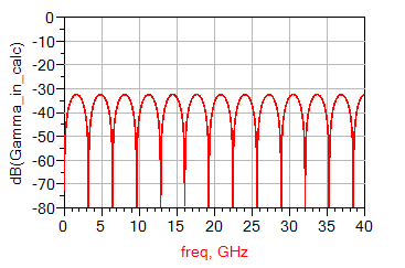
Figure 4. Input reflection coefficient of a lossless 51-Ohm transmission line in a 50-Ohm system, calculated with . The periodic behavior is due to the hyperbolic tangent function.
In other words, there will only be no reflections when all the impedances are identical: identically complex or identically real. Any impedance discontinuities in the system would invalidate and introduce periodic behavior to the return loss curve because of the hyperbolic tangent function.
Figure 4 illustrates the effect of the mismatch by calculating reflection coefficient of a lossless 51-Ohm line section in a 50-Ohm system with . A closer look at Figure 4 shows that the reflection coefficient reaches peaks and valley at specific frequencies depends on the length of the line; this frequency-preferential behavior is the signature of a resonator.

Figure 5. Looking from the input port and observing reflections from both ends of the line.

Having mathematically derived the resonance in mismatched transmission lines, we will take a different approach and examine the transmission line resonant behavior in a physical sense.
There will only be no reflections when all the impedances are identical; any slight impedance discontinuity introduces periodic behavior to the return loss curve. |
Figure 5 illustrates the impedance discontinuities when ZC is not matched to the source and load impedances. Observing from the input port (measuring S11), one would expect the reflections from the front end of the line where wave is transitioning from source impedance to the mismatched transmission line, and also from the back end of the line where wave transitions from mismatched transmission line to load impedance.
Analogous to the lumped element resonators, not only can the mismatched line be placed in series, a parallel connection is also possible.
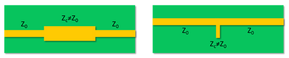
Figure 6. Left: top view of a series transmission line resonator. Right: top view of a parallel transmission line resonator.

Shown in Figure 6 are the two different transmission line configurations. In the series configuration, both ends of the mismatched line are connected to other transmission lines in the system. In the parallel case, however, only one end of the mismatched line is connected to the transmission line in the system, and the other end is usually left open.


Figure 7. Port assignment of the series resonator.
As illustrated in Figure 7, let the port on the left of the series resonator be the input port-port 1, and the port on the right of the series resonator be the output port-port 2. We will send sine waves of different frequency from the input port and monitor the received signal at the input port.
Since we know that there are two impedance mismatches, we can calculate the reflection coefficient at the junctions. Without loss of generality, we will take the impedance of the mismatched line, ZC, to be lower than 50 Ohms, i.e. ZC < Z0. In that case, the reflection coefficient at the front is

Figure 8. Assuming ZC is smaller than Z0, the reflection coefficient at the front is negative while the reflection at the back is positive.
as illustrated in Figure 8.

Figure 9. A reflected wave, Vr, and a transmitted wave, Vt, are created at the first discontinuity. The reflected wave changed its polarity because of the negative reflection coefficient.
Having established the reflection coefficients, we will first send a sine wave at a frequency where the length of the discontinuity, len,is a quarter of the wave length, i.e. len=λ/4.
The sine wave will travel forward from the input port to the first discontinuity. Encountered the first continuity, part of the wave is reflected with a negative reflection coefficient while part of the wave keeps travelling forward, towards port 2, as shown in Figure 9.
Define the first reflected backward travelling wave as Vr and the transmitted forward travelling wave as Vt, we can state that the forward travelling wave, Vt, will encounter the second discontinuity and be reflected after a quarter of a period, for the length of the mismatched line is a quarter of a wavelength.

Figure 10. The backward travelling Vt_r encounters the first discontinuity and is transmitted partially to the input port.

Figure 11. The transmitted forward travelling wave is reflected at the second discontinuity. However, the reflected wave does not change its polarity because of the positive reflection coefficient.
At the second discontinuity, part of Vt is reflected with a positive reflection coefficient while another part keeps travelling forward towards port 2. This voltage wave, Vt_r, is shown in Figure 11.
The electrical length of the discontinuity contributes to the delay the wave experiences. As frequency increases, the electrical length of a fixed length line also increases. |
With the defined backward travelling reflected Vt as Vt_r, we then state that it takes Vt_r another quarter of a period to reach the first discontinuity. Arrived the first discontinuity, Vt_r will again be reflected and transmitted. Since we are interested in what is coming to the input port, we will focus on the transmitted Vt_r, as shown in Figure 10.

Figure 12. The two waves at the input port add constructively and generate a peak voltage.
So far, at the input port, we have two waves, namely, Vr and Vt_r_t. Because of the negative reflection at the first discontinuity and the round trip, half a period delay, the two waves are in phase and add constructively to each other, resulting in a peak voltage at the input port, as shown in Figure 12.
This peak voltage also corresponds to the maximum mismatch between the input impedance looking into the first discontinuity and the system impedance.
Since a maximum reflected voltage is observed at the input port when the length of the discontinuity is a quarter of a wave length, the return loss, S11, of the system is also at its max. The constructive interference of the waves occurs as long as the Vt_r_t is half a period delayed when reaching then input port. Denote the time per period as Tp, we write,

When the electrical length of the mismatched line satisfies at different frequencies, S11 reaches peaks periodically as shown in our input reflection calculation.
Have stepped through the reflection of the waves to find physical reasons for the peaks in the return loss curve, one should be able to reason for the valleys as well. Instead of meticulously trace each reflection to understand the cause of the valleys, we will start with the two waves shown in Figure 12.

Figure 13. If the wave arriving at the first discontinuity is delayed by a full period. The sum of the two waves is at a minimum.
We observe that if the second wave, Vt_r_t, is to be delayed by exactly one period, the originally constructive interference becomes destructive, see Figure 13.
Consequently, the condition to have minimum voltage at the input port and lowest return loss is

For series resonators, when the electrical length of the discontinuity is a quarter of a wavelength, a maximum return loss is observed. If the discontinuity is half a wavelength, minimum return loss is observed. |
implies that when the electrical length of the discontinuity is a multiple of a half of a wave length, a minimum voltage is received at the input port, giving valleys, minimums, in the return loss curve.

Figure 14. Illustration of a parallel resonator with input port on the left and output port on the right.

Figure 14 demonstrates the setup for parallel resonator analysis. Again, let the port on the left of the parallel resonator be the input port-port 1, and the port on the right of the parallel resonator be the output port-port 2. We will monitor the input port while exciting the structure with a sine wave.
Looking at the first reflected wave, Vr, the analysis for parallel resonator with an open stub is not so different from the series resonator. As the wave travels down the line with impedance Z0, it reaches the T-junction where three transmission lines meet.
Looking at the first reflected wave, Vr, the analysis for parallel resonator with an open stub is not so different from the series resonator. As the wave travels down the line with impedance Z0, it reaches the T-junction where three transmission lines meet.

Figure 15. The first discontinuity seen by the wave is a width wider than the trace width of Z0. The resulting reflection coefficient is negative.
From the point of view of the wave, it first sees the constant trace width that makes Z0, but at the junction, it sees a combination of both ZC and Z0, a larger trace width than Z0 alone.
The larger width at the T-junction seen by the sine wave translates to a lower impedance compared to Z0, and results in a negative reflection coefficient, as shown in Figure 15.

Figure 16. Incident wave splits at the T-junction and goes down both paths. The wave in ZC path then reaches an open at the end of the stub and reflects.
At the junction, the transmitted sine wave splits into two and travel down both paths: the Z0 path and the ZC path. As the wave travels down to the end of ZC path, it sees an open circuit that has a positive reflection coefficient and reflects, as illustrated in Figure 16.

Figure 17. The wave reflected by the open travels back to the T-junction and splits into two waves. One travels towards the output port while another to the input port.
We will denote the wave that is first is transmitted and reflected by the open at the end of ZC branch as Vt_r. Been reflected by the open, Vt_r starts travelling back towards the T-junction. Although Vt_r is reflected and transmitted back at the T-junction, we focuses our attention on the transmitted wave that is travelling back to the input port, i.e. Vt_r_t, see Figure 17.
Because the wave has a finite speed, Vt_r_t would only make it to the input port after some time delay depending on the length of the stub. The situation at the input port is identical to that of the series resonator.
When the electrical length of the discontinuity (the stub in this case) is a quarter of a wave, Vt_r_t is delayed by half a period, so constructive interference takes place and maximum return loss is observed, On the other hand, when the electrical length of the stub is half of a wavelength, Vt_r_t is delayed by a full period, so destructive interference takes place and a minimum return loss is observed.

Figure 18. Location of two resonators on the Wild River Technology CMP-28 platform.

Figure 19. The series resonator to be measured on the Wild River Technology CMP-28 platform.
At the time of writing, both the series and resonant structures are available on the Wild River Technology [7]; therefore, instead of designing and fabricating a new board, we will take a look at measurement of a series and parallel resonator structures from the Wild River Technology Channel Modeling Platform, CMP-28 shown in Figure 18.
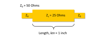
Figure 20. Illustration of the structure to be measured on the CMP-28 platform.
The structure to be measured (device under test, DUT) is shown in Figure 19. The series resonator itself is a 1-inch section of 25-Ohm line with ¼-inch 50-Ohm section on both ends, as illustrated in Figure 20.

Figure 21. Our measurement is a composite of two fixtures and the desired device under test.
Comparing Figure 19 and Figure 20, we find our measurement to be a composite measurement of a DUT/fixture combination, shown in Figure 21. Although the goal in any measurement is to extract an accurate value of the S-parameter of the device under test with minimum effort and artifacts, it is rarely the case the DUT is directly connected to the calibration plane of the instrument. To exclusively examine the DUT, one needs to isolate the performance of the fixture and use de-embedding techniques to “remove” the fixture from the measurements [8].
There are many techniques available for performing de-embedding, but not all provides scaling flexibility [9] [10]. To be able to fine-tune the fixture length and obtain a good model, the scalable measurement-based model (MBM) technique is implemented.

Figure 22. A 2X-Thru time domain impedance.
Generally, a 2X-thru structure that contains both fixture A and fixture B is measured. After imported the measurement, an EDA design tool is used to model the circuit and generate a measurement based S-parameter model of the fixture channel. Finally, the S-parameter models of the fixtures are bifurcated and placed in appropriate de-embed circuit elements to facilitate de-embedding calculation in the software.
Following the MBM de-embedding procedure, we first examine the 2X-thru measurement in the time domain to learn the impedance profile of the fixtures as in Figure 23.
In the modeling phase, fixture A and B are assumed to be identical, and transmission line segments of appropriate impedance are placed to match the measured profile. To get a good correlation of the loss performance of the fixture, frequency domain responses are also incorporated in the matching process.

Figure 23. Fixture model of the 2X-Thru.
After iterations of matching, a circuit model of the fixture consists of multiple sections of transmission lines is generated in Keysight ADS, see Figure 23.
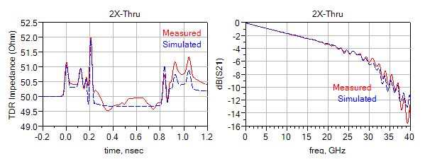
Figure 24. Correlation plots, and more words.
Shown in Figure 24are the impedance profile and the frequency domain response of the fixture model. The maximum impedance difference is within 2% of the measured impedance profile, while the insertion loss of the circuit model is within 1 dB of measurement up to 38GHz. After 38GHz, higher order modes of the connectors are introduced and cannot be modeled by simple transmission line sections [11].
To complete the MBM de-embedding process, the S-parameter of the fixture model is placed in 2-port de-embed blocks in schematics containing measurement of the resonators, as shown in Figure 26. Matrix transformation is initiated by the S-parameter de-embed blocks, which enables necessary computation to mathematically remove the fixtures in the measurement [12].

Figure 25. De-embedding block in Keysight ADS.
Using the knowledge learned from previous section, we can make a quick estimate on the frequency where return loss would peak. From , we know the first peak of return loss occurs when the electrical length of the discontinuity is a quarter of a wave length, corresponding to a physical length of 1 inch.
Knowing that a quarter of a wavelength is 1 inch, one can deduce that a full wavelength is 4 inches. Assuming the signal is propagating on a FR-4 substrate, the speed is therefore 6 inch/nsec. The frequency at the first peak of return loss is

Figure 26. Return loss measurement of the series resonator on CMP-28 shows a peak of return loss at 1.32GHz, in a reasonable range of our 1.5 GHz prediction.
Figure 26 shows measurement of return loss of the series resonator on the CMP-28 indicates the first peak to be located at 1.32GHz, consistent with our prediction from (18).

Figure 27. Parallel resonator to be measured on the CMP-28 platform. Although two stubs are present in this particular structure, the resonating behavior of the structure does no change.
Similar analysis is performed for the parallel resonator structure shown in Figure 27. Unlike the parallel resonator studied previously, the parallel resonator on the CMP-28 has two stubs of the same length at the junction. However, because the length of the two stubs are identical, waves reflected from both ends of the stubs would behave more or less the same way, so our analysis of a single stub still applies.

Figure 28. Illustration of the parallel resonator structure under test.
The construction of the structure is demonstrated in Figure 28. The CMP-28 parallel resonator has a 1-inch section of 50-Ohm connected to two 0.17 inch stubs in parallel followed by another 1-inch section of 50-Ohm.
The corresponding frequency for maximum return loss is calculated in the same fashion,

Figure 29. Return loss measurement of the parallel resonator on CMP-28 shows a peak of return loss at 7.8 GHz, in a reasonable range of our 8.8GHz prediction.
which is also reasonably close to the peak shown in the measurement of the parallel resonator, shown in Figure 29.
From the measurements of the resonators and their de-embedded counterparts, one learns the high frequency effect of the connectors and the importance of de-embedding.
At low frequencies, the connectors are electrically short so it does not contribute much to the measurement artifact. As frequency increases, the length of connectors gradually becomes compatible to a wavelength, and any discontinuities present in the connectors is interpreted as mismatch of the device under test.
De-embedding removes high frequency measurement artifacts introduced by the fixture leading to the device under test. |
To remove the artifact created by the connectors and to obtain the real measurement of the device under test, de-embedding is necessary step in the measurement process.
The Beatty Standard
In his years working in the field of microwave engineering, R. W. Beatty published numerous papers on accurate waveguide measurements and standards for waveguide calibration. It was not until 1972 that Beatty published a paper on a “new calculable standard of reflection coefficient and voltage standing wave ratio” that extends his tremendous microwave legacy to also reach modern signal integrity.
In the original Beatty standard, the waveguide standard consists of a quarter-guide-wavelength (λg/4) section of rectangular waveguide accurately constructed to have specified cross-sectional dimensions. These dimensions are chosen in a manner to be shown to give a desired calculable voltage-reflection coefficient or V.S.W.R. [13]. In use, the standard is terminated by a section of waveguide having the same nominal cross-sectional dimensions as has the output waveguide of the measuring system.
Although the signal integrity Beatty standard is structurally different than original one, the concept of using reflections to establish calibration values remains its central theme.
The Construction of Beatty Standard

Figure 30. Illustration of Beatty standard in signal integrity.
Used in signal integrity, the Beatty standard is a 1-inch transmission line that has trace width 3 times of a 50-Ohm line. To perform accurate material extraction (especially loss), the reference 50-Ohm termination is extended on each side of the Beatty standard so that impedances and losses of the two transmission lines of different trace widths are contributing to the measured data. To ensure a measurable amount of loss for a PCB structure, a standard 1 inch Beatty section is used, as shown in Figure 30.
Sensitivity Analysis of Beatty Standard
Fabricated on a printed circuit board, the Beatty standard is more than a series resonator. By building a virtual Beatty standard in Keysight ADS, we will analyze the effect different material properties has on the Beatty standard in time domain and in frequency domain. The sensitivity of the following material properties is examined,
Dk: dielectric constant of the substrate,
Df/TanD: dissipation factor or loss tangent of the substrate,
H: height of the substrate,
W: width of the traces,
σ: the conductivity of the printed copper.
Starting Point-Ideal Lossless Line
To set a simulation base line, an ideal lossless strip line Beatty standard is simulated. The material properties used in ADS model is listed in Tables 1 and the schematic setup is shown in Figure 32.
|
Parameter |
Initial value |
Unit |
|
Dk: Dielectric constant |
4 |
- |
|
Df: Loss tangent |
0 |
- |
|
H: Height of substrate |
10 |
mil |
|
W: Width of 50 Ohm trace |
7.4 |
mil |
|
σ: Conductivity |
1050 |
S/m |
Table 1. Initial input values for ideal lossless Beatty standard.

Figure 31. Schematic setup for ideal lossless Beatty standard simulation.

Figure 32. Simulation result of ideal lossless Beatty standard.
With the setup shown, we expect the impedance profile to start at very close to 50 Ohms and drops down to a lower value at 0.17 nsec because the wider trace. The insertion loss curve should have ripples because of the mismatched line in the middle. However, since both conductor loss and dielectric loss are not present in the simulation, there should be no difference between one peak and another as frequency increases.
Although simulation results are consistent with our expectation as shown in Figure 33, there is an unexpected 47-Ohm impedance at 0.5 nsec. The 47-Ohm impedance should not be alarming since it is an artifact created by the reflection from the discontinuity from the other end of the line.
Dielectric Constant Variation

Figure 33. Impedance profile with Dk variation.
As we change the dielectric constant, we expect with higher Dk value, the impedance is lower while a lower Dk results in a higher impedance. Nevertheless, we do not expect the impedance of all three transmission lines to change the same amount, for capacitance of a wider trace is less sensitive to dielectric constant than a narrower line. Consequently, we would expect the impedance change be larger in the 50-Ohm lines than the three-times-wider Beatty line, as shown in Figure 34.

Figure 34. Phase Delay plot from different Dk values. Lower Dk corresponds to a lower time delay.
On the other hand, we expect the delay to be larger when the dielectric constant is larger because the delay is proportional to the square root of dielectric constant. In Figure 35, the order of the lines is opposite of the ones shown in the impedance plot, indicating a different relationship.

Figure 35. Impedance profile of different loss tangent values. Larger loss tangent corresponds to higher loss and lower positive reflection at 0.6 nsec.
Loss Tangent Variation
As we introduce loss tangent in the system, we would expect some of the signal to be dissipated as heat. The result of less signal coming back translates into less reflections. The reflection from the end of the Beatty line is a good indicator for the loss. As shown in Figure 36, at 0.6 nsec, as the tangent loss increases, less and less positive reflection is in place to keep the curve close to the ideal lossless case.

Figure 36. Insertion loss curves showing frequency-dependent dielectric loss.
More importantly, since dielectric loss is linear proportional with frequency, we should see an obvious drop-off of insertion loss at higher frequency, as shown in Figure 37.

Figure 37. Situating on the same substrate, all the impedance changes about the same amount when the height of the substrate is changed.
Substrate Height Variation
Unlike changing the dielectric constant where width of the traces affects the amount of change, changing substrate height results in a uniform impedance change in the three section of lines since they all situate on the same substrate, shown in Figure 38.
The impedance change of the transmission lines, in turn, causes more reflections in the system, so we expect the valley of ripples in insertion loss to get worse. Figure 39 shows simulation result consistent with our expectation.

Figure 39. An identical, small width change affects narrower lines more significantly than the wider lines.
Trace Width Variation
By introducing a small delta value to signify the overall etch-back or over-plate of copper, we can show the influences of such fabrication inevitability. Because we have designed the width of the Beatty section to be exactly three times wider than the 50-Ohm line, we expect to see a smaller variation in impedance in the Beatty section, as shown in Figure 40.
As reasoned in the substrate height variation section, the impedance change of the lines will also affect the ripples in the insertion loss curve. Although not as dramatic as in the substrate height, we can still see the mismatch worsen in Figure 41.

Figure 40. Slight width change creates more mismatch and is again manifested in the ripple of the insertion loss.
Conductivity Variation

Figure 41. Finite copper conductivity is seen by the signal as series resistance that increases the impedance of the lines.
Conductor loss in copper presents itself as series resistance in the impedance profile. Therefore, if we decrease the conductivity of copper from ideally infinite to a finite number, we will see an increase of impedance. Five different conductivity values ranging from 5 MS/m to 6 MS/m are used to simulate Figure 42. The impedance profile of the five different conductivities are quite similar.
Although not increasing linearly as frequency increases, the conductor loss is proportional to the square root of frequency, so we can still expect a certain amount of drop-off in the insertion loss graph, see Figure 43.

Figure 42. Conductor loss causes a small drop-off of insertion loss at high frequency.
The distinct response of each parameter is a signature that help to extract the as-fabricated material properties. |

Figure 43. De-embedded Beatty measurement.
Material Property Extraction with the Beatty Standard
The material property extraction process is based on a good understanding of the effect each material parameter has on different aspect of the simulated curves. Having removed the launches and transmission lines, we obtain the true Beatty standard measurement, shown in Figure 44.
We perform the analysis by first assume a set of as-designed material properties, values seen on a schematic and dimensions found on layout. We address these as-designed properties with subscript “d.” In the real world, the fabricated board is never exactly the same as the as-designed one. After the numerous steps of chemical and mechanical fabrication process, the as-fabricated parameters are inevitably different from the ones designed. With subscript “f,” we differentiate the as-fabricated material properties from the as-designed ones. The relation between the designed parameters and the fabricated ones is

The delta quantity indicates the amount of change of each parameter in the fabrication process. The delta quantities are varied in the sensitivity analysis to demonstrate how the fabrication process change the different response of the structure.
|
Parameter |
As-designed Value |
Unit |
|
Dk: Dielectric constant |
3.68 |
- |
|
Df: Loss tangent |
0.0072 |
- |
|
H1: Height of top substrate |
12 |
mil |
|
H2: Height of bottom substrate |
10 |
mil |
|
W: Width of 50 Ohm trace |
11 |
mil |
|
σ: Conductivity |
5.8∙107 |
S/m |
Table 2. As-designed values for each of the material parameters

Figure 44. Simulation with as-designed parameters in Table 2.
Using the as-designed values shown in Table 2, we perform a preliminary simulation to begin the extraction process. We see in Figure 45that with the as-designed parameters, the simulated impedance is uniformly lower that the measured, and the insertion loss at high frequency is not as low as the measured one. According to the two clues, we need to increase the substrate height and loss tangent to match the impedance and the loss. After changing the height of the substrate and the loss tangent, we also fine tune the dielectric constant by examining the delay.

Figure 45. Matching simulation to measurement to find as-fabricated material properties.
As frequency increases above 30 GHz to involve the higher order modes of the connectors, the measurement and simulation would be expected to be different, for we had not included resonant modes of the connectors in our model, as shown in Figure 46.
Nonetheless, we still have confidence in our as-fabricated material properties up to 30 GHz. Table 3shows a comparison between the as-designed values and extracted as-fabricated values. Notice that in the extraction process the as-fabricated values are kept at the same order of magnitude of the as-designed values, so a realistic model can be generated.
|
Parameter |
As-designed Value |
Delta |
As-fabricated |
Unit |
|
Dk: Dielectric constant |
3.68 |
0.026 |
3.706 |
- |
|
Df: Loss tangent |
0.0072 |
0.005 |
0.0132 |
- |
|
H1: Height of top substrate |
12 |
1 |
13 |
mil |
|
H2: Height of bottom substrate |
10 |
1 |
13 |
mil |
|
W: Width of 50 Ohm trace |
11 |
0.2 |
11.2 |
mil |
|
σ: Conductivity |
5.8∙107 |
0 |
5.8∙107 |
S/m |
Table 3. Comparison between as-designed values and extracted as-fabricated values.

Having extracted the as-fabricated material properties in, we validate the information by creating a model for a parallel stub and perform simulation with the as fabricated values. Shown in Figure 47is the schematic setup of the stub resonator simulation; the lengths of the stubs and peripheral transmission lines are found in the layout, and no other modification is made.

Figure 47. Extracted substrate definition used in simulating the stub resonator.
The corresponding extracted substrate definition is shown in Figure 48.

Figure 48. Simulation of a stub resonator using the as-fabricated material properties.
Simulation result is shown in Figure 48; aside from the artifact above 30 GHz, the as-fabricated substrate model correctly predicted the loss and impedance.
Summary
It is not a simple task to match simulation to measurement, but there are ways to reduce the complexity. In the design process, it is beneficial to include a reference fixture structure so that the device under test can be correctly identify with de-embedding. With a properly de-embedded measurement of the DUT, one needs special standards to extract the as-fabricated material properties: the Beatty standard.
By matching a simulated Beatty standard model to a de-embedded measurement, valuable information about the substrate and trace can be extracted. By practicing engineering judgment and with enough experience with the Beatty standard, matching simulation and measurement can be done accurately and with confidence.
The use of Beatty standard is not limited to matching simulation to measurement. To manufactures, the material properties extracted from the Beatty standard can be used as a tool to examine the quality and consistency of the fabrication process.
References
|
[1] |
"IPC-TM-650 TEST METHODS MANUAL," September 2009. [Online]. Available: http://www.ipc.org/4.0_Knowledge/4.1_Standards/test/2-5_2-5-5-12.pdf. |
|
[2] |
D. DeGroot, P. Pupalaikis and B. Shumaker, "Total Loss: How to Qualify Circuit Boards," in DesignCon, Santa Clara, 2011. |
|
[3] |
M. R. Harper, N. M. Ridler and M. J. Salter, "A Proposed Standard for Loss Measurements on Printed Circuit Boards," in 3rd Annual Seminar on Passive RF and Microwave Components, 2012. |
|
[4] |
A. Rajagopal, B. Achkir, M. Koledintseva, A. Koul and J. Drewniak, "Material parameter extraction using Time-Domain TRL (t-TRL) measurements," in IEEE International Symposium on Electromagnetic Compatibilit. |
|
[5] |
H. Barnes, R. Schaefer and J. Moreira, "Analysis of test coupon structures for the extraction of high frequency PCB material properties," Signal and Power Integrity (SPI), 2013 17th IEEE Workshop on, May 2013. |
|
[6] |
E. Gago-Ribas, C. Dehesa-Martinez and M. J. Gonzalez-Morales, "Complex Analysis of the Lossy-Transmission Line: A Generalized Smith Chart," Turkish Journal of Electrical Engineering & Computer Sciences, vol. 14, no. 1, pp. 173-194, 2006. |
|
[7] |
Wild River Technology, "CMP-28 Channel Modeling Platform," Wild River Technology, 2015. [Online]. Available: https://wildrivertech.com/cmp-28cmp-32-channel-modeling-platforms. |
|
[8] |
Agilent Technologies, "The ABCs of De-Embedding," 2007. |
|
[9] |
J. Carrel, R. Sleigh, H. Barnes, H. Hakimi and M. Resso, "Tips and Advanced Techniques for Characterizing a 28 Gb/s Transceiver," in DesignCon, Santa Clara, 2013. |
|
[10] |
L. Ritchey, H. Barnes, T. Wang Lee and A. Neves, "Breaking the 32 Gb/s Barrier: PCB Materials, Simulations and Measurements," in DesignCon, Santa Clara, 2015. |
|
[11] |
The Institution of Engineering and Technology, "Connectors, air lines and RF impedance," in Microwave Measurements, London, The Institution of Engineering and Technology, 2007, pp. 179-188. |
|
[12] |
Agilent Technologies, "De-embedding Techniques in Advanced Design System," Agilent Technologies. |
|
[13] |
R. W. Beatty, "2-Port lamda/4 Waveguide Standard of Voltage Standing-Wave Ratio," Electronics Letters, vol. 9, no. 2, pp. 24-26, 25 January 1972. |
|
Figure 5. Looking from the input port and observing reflections from both ends of the line. |
|
Figure 5. Looking from the input port and observing reflections from both ends of the line. |