Permittivity is the ability of a dielectric material to store electrical energy in an electric field. In the PCB industry, relative permittivity (εr) and effective relative permittivity (εreff) are synonymous with dielectric constant (Dk) and effective dielectric constant (Dkeff) respectively. Herein, Dk and Dkeff are substituted accordingly.
By definition [6], Dkeff is the ratio of the actual structure`s capacitance to the capacitance when the dielectric is replaced by air. When modeling lossy transmission lines, using manufacturers’ published dielectric and conductor material properties, often leads to a discrepancy in Dkeff due to increased phase delay caused by surface roughness. This often leads to inaccuracy in simulated insertion loss (IL), as shown in the example of Figure 1 left. But when Dkeff is tuned to measured value instead, the accuracy of IL is often improved, as shown on the right.

Figure 1. Simulated vs measured results for insertion loss and Dkeff vs frequency using manufacturers’ data sheet parameters (left) and when Dkeff was tuned to measured value at 10 GHz (right). Modeled and simulated with Keysight EEsof EDA ADS [15].
Phase delay, also known as time delay (TD), is the time it takes for a signal to propagate from one end of a transmission line to the other. It can be derived from the transmission S(2,1) phase angle of the S-parameter.
In an IEEE paper [3], the authors observed an increase in phase delay proportional to roughness profile and dielectric material thickness. This would explain why there is often difference between simulated and empirical results.
The motivation for this research work was to try and develop a method to accurately predict Dkeff and phase delay due to conductor surface roughness profile, as published in manufacturers’ data sheets, without relying on measured data for curve fitting.
Background
Effective Dk can be derived from TD, and is often used as a metric for simulation correlation accuracy instead. TD, as a function of frequency, in seconds, is calculated from the unwrapped measured transmission phase angle, and is given by [4]

Where:
c = speed of light (m/s);
Length = length of conductor (m).
Since TD is proportional to relative permittivity of the material, my theory is the surface roughness profile decreases the separation between the reference plane(s) and conductor, thereby increasing the electric field (e-field) strength, resulting in additional capacitance, which accounts for an increase in effective Dk and phase delay.
The main focus of this paper is to prove the theory and to show a practical method to model effective Dk and phase delay due to surface roughness. By referencing Gauss’s Law for charged parallel plates, I show mathematically, and through simulation, how the dielectric thickness and permittivity are interrelated to e-field and capacitance. I also reveal how the 10-point mean (Rz) roughness parameter is applied to finally determine effective Dk due to roughness, and then test the model via case studies.
Application of Gauss’ Law
Gauss’ law relates the distribution of electric charge to resulting e-field, and can be used to determine the e-field between two large and oppositely charged parallel plates. Referring to Figure 2, the e-field in free space (E0), is equal to the ratio of the charge density (σ), to the permittivity of free space (ε0), and is given by [5]:
Equation 3
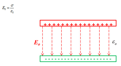
Figure 2. Electric field between two large and oppositely charged parallel plates in free space.
Dielectric materials are insulators often composed of polar molecules. These molecules look electrically like small dipoles with a negative charge on one end and positive charge on the other. In the absence of an external electric field, these molecules line up randomly as shown in Figure 3.

Figure 3. Random distribution of dipoles in the absence of an electric field.
When a dielectric material is placed between two, large and oppositely charged parallel plates, the dipoles align as shown in Figure 4. The collective e-field of the dipoles (ED) opposes the e-field in the absence of any dielectric (E0) to yield a net e-field intensity (E).
Equation 4

Figure 4. Polarization of dipoles in the presence of an electric field between two large and oppositely charged parallel plates.
Since the insertion of dielectric material reduces the e-field intensity inversely proportional to the Dk of the material, the e-field intensity E is given by [5]:
Equation 5

If charge density (σ) is defined as the charge (Q), per unit area (A), of a surface, then E is given by [5]:
Equation 6

Electric Field vs Parallel Plate Separation
Electric field intensity can also be expressed as the ratio of the potential difference in volts (V), to the distance (d) between two plates, and is given by [5]:
Equation 7

Referring to Figure 5, since electric field intensity is inversely proportional to the distance between two large parallel plates, with constant voltage, it can be shown that by applying Equation 7, the ratio of E2 to E1 is:
Equation 8

Figure 5. Illustration showing electric field intensity (E) is inversely proportional to the separation (H) between two oppositely charged parallel plates, with constant voltage.
Parallel Plate Capacitor
Any structure capable of storing an electric charge is called a capacitor. Figure 6 is an example of such a structure. The relationship between capacitance, voltage, separation and charge is given by [5]:
Equation 9
Where:
C is capacitance in farads (F)
Q is charge on either conductor in coulombs (C)
V is potential difference between charges in volts
Dk is the dielectric constant of the material
ε0 is permittivity of free space (~ 8.85pf/m)
A is the area of the plates (m2)
H is the separation between plates (m)
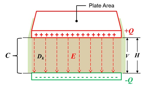
Figure 6 Two equally large and oppositely charged parallel plates, closely separated by a dielectric, forms a capacitor.
Since capacitance is inversely proportional to the separation between two, large and oppositely charged parallel plates, with constant voltage, it can be shown that by applying Equation 9, the ratio of C2 to C1 is:
Equation 10

Conductor Surface Roughness
Rolled and electro-deposited (ED) are two copper foil fabrication processes used in PCB laminate construction today. Of the two, rolled copper will always be smoother than standard ED copper.
ED copper is widely used in the printed circuit (PCB) industry. It is produced by electro-depositing copper, from a bath of copper sulfate solution, onto a large rotating drum made of stainless steel or titanium. The speed of the drum rotation determines the thickness of the foil.
A finished sheet of ED copper foil has a matte side and drum side. The matte side is the side facing the copper sulfate solution while the drum side faces the drum surface. The drum side is always smoother than the matte side.
The matte side is usually bonded to the core laminate. For high-speed boards, the drum side of the foil is sometimes laminated to the core instead. In that case it is referred to as reversed treated (RT) foil.
Profilometers are often used to quantify the roughness tooth profile of ED copper. Figure 7 shows an example profile of a rough conductor surface. Tooth profiles are typically reported in terms of 10-point mean roughness for both sides, but sometimes the drum side reports average roughness in manufacturers’ data sheets if there is very little roughness. Some manufacturers may also report root-mean-square (RMS) roughness (Rq).
The10-point mean (Rz), is the sum of the average of the five highest peaks and the five lowest valleys, of the rough conductor surface over the sample length. The average surface roughness parameter (Ra) is the arithmetic average of the roughness profile over the sample length.

Figure 7. Schematic illustration of a rough conductor profile as measured with a profilometer.
Effective Dk Due to Roughness
In an IEEE paper [3], the authors observed an increase in Dkeff proportional to the conductor roughness profile and inversely proportional to dielectric material thickness. Figure 8 plots Dkeff vs dielectric height for Rogers LCP dielectric material with two foil roughness profiles.

Figure 8. Extracted Dkeff vs. thickness for 50 ohm transmission lines on LCP clad with 0.4 and 3.0 μm profile foils [3].
It was observed that for a relatively smooth copper profile with Rq = 0.4μm, Dkeff pretty much matched the manufacturer’s published value of 3. But when a rougher copper profile with Rq = 3.0 μm was used, it revealed two things:
- As thickness of the dielectric increased from 5 mils to 20 mils, Dkeff decreased.
- The rougher the copper profile, the higher Dkeff for the same dielectric thickness.
This supports the theory that the higher roughness profile adds additional capacitance, thereby increasing Dkeff, due to reduced separation between the two large parallel plates, and can be explained with the aid of Figure 9.
The illustration on the left shows two smooth copper foil sheets bonded to each side of a dielectric material. The separation is denoted by Hsmooth and is equal to thickness tdiel. On the right shows two copper foil sheets with an exaggerated roughness profile, attached to the same thickness of dielectric material. Both copper sheets have the same thickness with roughness included, but now the effective separation is reduced, as denoted by Hrough.
This is because curing of the prepreg into a core, under heat and pressure, sees the rough copper tooth profile being pressed into the prepreg. As a result, the effective separation between copper sheets is less, compared to smooth copper.
In the PCB industry, prepreg is the term commonly used to describe a weave of glass fiber yarns pre-impregnated with resin which is only partially cured. Since Rz is a 10-point mean metric of the roughness profile, we can assume the effective separation reduces proportionally to a mean height of Hrough , and therefore the average capacitance will increase proportionally.

Figure 9. Smooth and rough copper foil sheets bonded to dielectric material. Capacitance increases in proportion to roughness profile Rz.
Quickfield modeling software [18] was used to simulate and verify the theory. The results are shown in Figure 10. The figure on the left shows two smooth copper foil sheets bonded to the top and bottom of a 2 cm thick dielectric material.
A Dk of 4.0 was used for the permittivity, and a +1.0 V potential was applied between the top and bottom plates respectively. As expected the e-field strength was uniform throughout. The capacitance reported by the software wizard was 141.67 pF/m.
On the right shows two copper foil sheets, with an exaggerated roughness profile, attached to the same thickness and properties of dielectric material. The peak-peak thickness of each plate is equal to the thickness of respective smooth plate.
When +1.0 V potential was applied, the e-field strength increased, or decreased in proportion to the roughness peaks and valleys of the roughness profile respectively. The average capacitance increased to 175.99 pF/m.

Figure 10. Quickfield [18] simulation of smooth vs rough conductor with same thickness of dielectric. With smooth plates, as shown on the left, the e-field strength is uniform, as expected. The roughness profile, as shown on the right, increases or decreases the e-field strength proportional to the peaks and valleys respectively. Average capacitance also increases proportionally to the roughness profile.
Modeling Effective Dk Due to Roughness
Wadell [6] defines Dkeff as the ratio of the actual structure's capacitance to the capacitance when the dielectric is replaced by air.
Equation 11

Dkeff is highly dependent on the test apparatus and conditions of how it is measured. There are several methods used in the industry, as referenced in [7]. One method, commonly used by many laminate suppliers, is a clamped stripline resonator test method, described by IPC-TM-650 Test Methods Manual [8].
IPC-TM-650, section 2.5.5.5, Rev C, defines test methods to rapidly test dielectric material for permittivity and loss tangent, over an X-band frequency range of 8-12.4 GHz, in a production environment.
The measurements are made under stripline conditions using a carefully designed resonant element pattern card, made out of the same dielectric material to be tested. The card is sandwiched between two sheets of unclad dielectric material under test. The whole structure is then clamped between two large plates, lined with copper foils that are grounded. They act as reference planes for the stripline.
By measuring a resonant frequency of the cavity, the effective permittivity and loss tangent are determined, as outlined in [8]. The value of this method is to assure consistency of product, when used in fabricated boards. It does not guarantee the values directly correspond to design applications.
This is a key point to keep in mind, and here is why.
Since the resonant element pattern card and material under test are not physically bonded together, as it would be the case in real life, there are small air gaps between the various layers that affect measured results. These air gaps are caused, in part, by:
- Etching away the copper on material under test, leaving the bare substrate complete with the micro void imprint of the copper roughness.
- The air gap between resonant element pattern card and material under test due to the copper thickness of the etch pattern.
- The roughness profile of the copper, on the resonant element pattern card and fixture’s grounded foil reference planes, are different than would likely be in practice. Empirical results from [3] would suggest that very smooth, copper foil was likely used for the test fixture.
If Dkeff and Rz roughness parameters from the manufacturers’ data sheets are known, then the effective Dk due to roughness of the fabricated core laminate can now be easily determined as follows †:
Given:

Where:
Dkeff is the Dk of the dielectric material as published in manufacturer’s data sheet.
Hsmooth is the thickness of the dielectric as published in manufacturer’s data sheet.
Hrough is the effective height between plates due to roughness profile. If Rz is used for the height of the roughness profile, then separation between copper plates Hrough is:
Equation 12

With reference to Figure 11, using Dkeff with rough copper model, as shown on the left, is equivalent to using Dkeff_rough with smooth copper model, as shown on the right. Therefore Dkeff_rough would be used for impedance calculation and numerical simulations based on surface roughness, instead of effective Dk value published in manufacturers’ data sheets.

Figure 11. Effective Dk due to roughness model. Using Dkeff with rough copper model (left) is equivalent to using Dkeff_rough with smooth copper model (right).
Validating the Model over Dielectric Height
When applying Equation 15 to results of IEEE paper [3], and initially tuning Rz equal to 6.1 μm at 4 mil dielectric height, then using that value for the other dielectric heights, there is excellent correlation to measured Dkeff , as shown in Figure 12.

Figure 12. Measured [3]vs simulated Dkeff of rough copper profile when dielectric height is varied from 4 mils to 20 mils.
FR408HR - RTF Case Study
To test the accuracy of the model, board parameters and measured data from [10] was used. The extracted de-embedded generalized modal S-parameter (GMS) data was computed from 2 inch and 8 inch single-ended stripline traces. They were originally measured from the CMP-28 40 GHz High-Speed Channel Modeling Platform [11], and provided by [14].
The PCB was fabricated with Isola FR408HR material. The default foil is MLS, Grade 3, controlled elongation RTF. Roughness Rz parameters for drum and matte sides are 120μin (3.048 μm) and 225μin (5.715μm) respectively for 1 oz. copper [13].
An oxide or micro-etch treatment is usually applied to the copper surfaces prior to final lamination. The etch treatment creates a surface full of micro-voids which follows the underlying rough profile and allows the resin of the prepreg to squish in and fill the voids, providing a good anchor. Typically 50 μin (1.27μm) of copper is removed when the treatment is completed, depending on the board shop’s process control.
The PCB stripline geometry physical parameters are shown in Figure 13. H1, H2 and t are thicknesses of core, prepreg and copper foil respectively, as published in manufacturers’ data sheets. Widths w1 and w2 are the design specific parameters for the bottom and top surfaces of the PCB trace respectively.
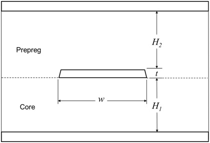
Figure 13. Generic PCB stripline geometry showing core, prepreg, dielectric heights and conductor parameters.
The data sheet and design parameters are summarized in Table 1. Respective Dk, Df, core, prepreg and trace thickness were obtained from the isoStack® software [12]. Roughness of the matte side after micro-etch treatment (Rz = 4.445μm) was used to determine Dkeff of the prepreg.
Table 1 FR408HR test board parameters obtained from manufacturers’ data sheets and design objective.
|
Parameter |
FR408HR/RTF |
|---|---|
|
Dk Core/Prepreg |
3.65/3.59 @10GHz |
|
Df Core/Prepreg |
0.0094/0.0095 @ 10GHz |
|
Rz Drum side |
3.048 μm |
|
Rz Matte side before Micro-etch |
5.715 μm |
|
Rz Matte side after Micro-etch |
4.445 μm |
|
Trace Thickness, t |
31.730 μm |
|
Trace Etch Factor |
2:1 (60 deg taper) |
|
Trace Width, w |
11 mils (279.20 μm) |
|
Core thickness, H1 |
12 mils (304.60 μm) |
|
Prepreg thickness, H2 |
10.6 mils (269.00 μm) |
|
GMS trace length |
6 in (15.23 cm) |
By applying Equation 15, determine Dkeff of core and prepreg due to roughness:
- Dkeff_core :

- Dkeff_prepreg :

Keysight EEsof EDA ADS software [15] was used for modeling and simulation analysis. The controlled impedance line (CIL) model allows modeling of trapezoidal traces.
Figure 14 is the general schematic used for analysis. There are three transmission line substrates; one for dielectric loss; one for conductor loss and the other for total loss without roughness.
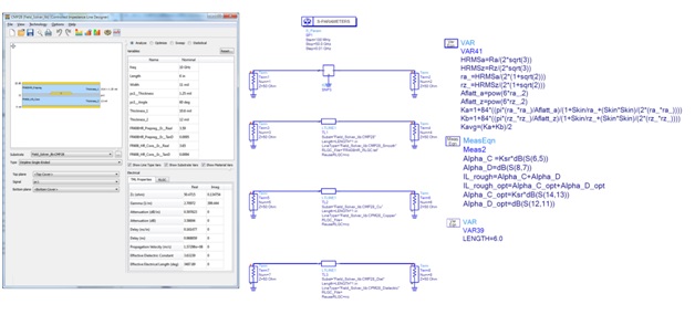
Figure 14. Keysight EEsof EDA ADS [15] generic schematic of controlled impedance line designer used in the modeling and simulation analysis.
Dielectric loss was modeled using the Svensson/Djordjevic wideband Debye model to ensure causality. By setting the conductivity parameter to a value much-much greater than the normal conductivity of copper ensures the conductor is lossless for the simulation. Similarly the conductor loss model sets the Df to zero to ensure lossless dielectric.
Conductor loss due to roughness was modeled using cubic close-packing of equal spheres (CCPES) model, and total insertion loss was determined as described in [10].
Results
Results for effective permittivity due to roughness are shown in Figure 15. On the left graph, Dkeff measured (red) was 3.761 compared to simulated Dkeff (blue) of 3.626, at 10 GHz, when data sheet values for core and prepreg were used. This gave an error of -3.6%.
But when the respective Dkeff_rough was used for core and prepreg there was better correlation, Dkeff =3.727vs 3.761, for an error of only -0.9%, as shown on the right graph.
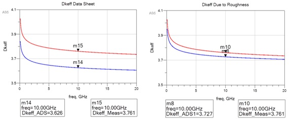
Figure 15. Measured vs simulated Dkeff using FR408HR data sheet values for core and prepreg (left) and using Dkeff_rough (right).
Simulated IL and phase delay, due to conductor roughness, are shown in Figure 16. The left graph compares measured IL and phase delay (red) vs simulated (blue) when data sheet parameters were used. IL are the top curves and phase delay are bottom curves. The right graph shows improved phase delay over the entire frequency range and IL improvement past 25GHz when respective Dkeff_rough was used for core and prepreg.

Figure 16. Simulated results for insertion loss (top curves) and phase delay (bottom curves) using FR408HR data sheet values for Dkeff (left graph) and using Dkeff_rough (right graph). Measured results are red curves and simulated are blue.
N4000-13EP/VLP Case Study
The PCB stripline geometry parameters are the same as shown in Figure 13. Table 2 summarizes parameters from DesignCon 2015 Paper [9] and material data sheets. Material was N4000-13EP with very low profile (VLP) foil. Respective Dk, Df, core and prepreg values were obtained from Nelco dielectric calculator software [17].
Table 2 N4000-13EP test board parameters obtained from manufacturers’ data sheets and design objective.
|
Parameter |
N4000-13EP/RTF |
|---|---|
|
Dk Core/Prepreg |
3.83/3.72 @10GHz |
|
Df Core/Prepreg |
0.0085/0.0085 @ 10GHz |
|
Rz Matte side |
2.50 μm |
|
Ra Drum w/ Micro-etch |
1.44 μm |
|
Trace Thickness, t |
15.23 μm |
|
Trace Etch Factor |
2:1 (60 deg taper) |
|
Trace Width, w |
9.9 mils (251 μm) |
|
Core thickness, H1 |
9.8 mils (249 μm) |
|
Prepreg thickness, H2 |
9.09 mils (231 μm) |
Similar to CMP-28 case study, the same method using Keysight EEsof EDA ADS software [15] was followed for modeling and simulation analysis. Equation 15 was used to determine Dkeff of core and prepreg due to roughness. Dielectric loss was modeled using the Svensson/Djordjevic wideband Debye model to ensure causality. Conductor loss due to roughness was modeled using hexagonal close-packing of equal spheres (HCPES) model, as described in [9].
Results
Results for effective permittivity due to roughness are shown in Figure 17. On the left graph, Dkeff measured (red) was 3.867 compared to simulated Dkeff (blue) of 3.792, at 10 GHz, when data sheet values for core and prepreg were used. This gave an error of -1.9%.
But when the respective Dkeff_rough was used for core and prepreg there was better correlation, Dkeff =3.829 vs 3.867, for an error of only -0.98%, as shown on the right graph.
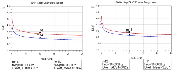
Figure 17. Measured vs simulated Dkeff using N4000-13EP data sheet values for core and prepreg (left) and using Dkeff_rough (right).
Simulated IL and phase delay, due to conductor roughness, are shown in Figure 18. The left graph compares measured IL and phase delay (red) vs simulated (blue) when data sheet parameters were used. IL are the top curves and phase delay are bottom curves. The right graph shows slight improvement in IL and phase delay when respective Dkeff_rough was used for core and prepreg.

Figure 18. Simulated results for insertion loss (top curves) and phase delay (bottom curves) using N4000-13EP data sheet values for Dkeff (left graph) and using Dkeff_rough (right graph). Measured results are red curves and simulated are blue.
As expected, there was not a dramatic impact in either Dkeff or phase delay, compared to FR408HR/RTF case study, because VLP foil is typically smoother than RTF foil and is consistent with the study done by[3].
Summary and Conclusions
- Analysis done in this paper supports the theory that surface roughness profile decreases the separation between the reference plane(s) and conductor, thereby increasing the e-field strength, resulting in additional capacitance, which accounts for increased Dkeff and phase delay as summarized by:

- By using an effective Dk due to roughness, derived from Gauss’ Law for parallel plate capacitors, instead of published Dk values from data sheets, excellent results were achieved, when compared to measured data without curve fitting.
Acknowledgements
I would like to thank the following people for their support in completing this study.
- Dr. Alexandre Guterman for reviewing and making constructive suggestions to this paper.
- Dr. Eric Bogatin for candid discussions and sharing his insights in the beginning of this research study.
References
1. E. Bogatin, "Signal Integrity Simplified", Prentice Hall PTR, 2004.
2. Huray, P. G. (2009) "The Foundations of Signal Integrity", John Wiley & Sons, Inc., Hoboken, NJ, USA., 2009
3. A. F. Horn, J. W. Reynolds and J. C. Rautio, "Conductor profile effects on the propagation constant of microstrip transmission lines," Microwave Symposium Digest (MTT), 2010 IEEE MTT-S International, Anaheim, CA, 2010, pp. 1-1.doi: 10.1109/MWSYM.2010.5517477
4. E. Bogatin, D. DeGroot, P.G. Huray, Y.Shlepnev, "Which one is better? Comparing Options to Describe Frequency Dependent Losses," DesignCon 2013, vol. 1, 2013, pp. 469-494
5. P. E. Tippens, "Applied Physics", McGraw-Hill Inc., 1973.
6. Brian C Wadell, Transmission Line Design Handbook, Artech House, Inc., 1991.
7. G. Oliver, J. Weldon , C. Nwachukwu, J. Andresakis, J. Coonrod, D. L. Wynants Sr., D. DeGroot, "Round Robin of High-Frequency Test Methods by IPC-D24C Task Group (Part 1)", The PCB Magazine , July 2016
8. IPC-TM-650, 2.5.5.5, Rev C, Test Methods Manual, "Stripline Test for Permittivity and Loss Tangent (Dielectric Constant and Dissipation Factor) at X-Band", 1998
9. B.Simonovich, "Practical Method for Modeling Conductor Surface Roughness Using Close Packing of Equal Spheres", DesignCon 2015 Proceedings, Santa Clara, CA, 2015
10. B.Simonovich, "Practical Model of Conductor Surface Roughness Using Cubic Close-packing of Equal Spheres", EDICon 2016, Boston
11. Wild River Technology LLC 8311 SW Charlotte Drive Beaverton, OR 97007. URL: http://wildrivertech.com/home/
12. Isola Group S.a.r.l., 3100 West Ray Road, Suite 301, Chandler, AZ 85226. URL: http://www.isola-group.com/
13. Oak-mitsui 80 First St, Hoosick Falls, NY, 12090. URL: http://www.oakmitsui.com/pages/company/company.asp
14. Simberian Inc., 3030 S Torrey Pines Dr. Las Vegas, NV 89146, USA,
15. Keysight Advanced Design System (ADS) [computer software], (Version 2016). URL: http://www.keysight.com/en/pc-1297113/advanced-design-system-ads?cc=US&lc=eng.
16. W. Beyene, Y.-C. Hahm, J. Ren, D. Secker, D. Mullen, Y. Shlepnev, "Lessons learned: How to Make Predictable PCB Interconnects for Data Rates of 50 Gbps and Beyond", DesignCon2014
17. Park Electrochemical Corp. Nelco Digital Electronic Materials
18. Quickfield Student, Terra Analysis Ltd., Version 6.2.0.1828 URL: http://www.quickfield.com/index.htm
Author Biography
Lambert (Bert) Simonovich graduated in 1976 from Mohawk College of Applied Arts and Technology, Hamilton, Ontario Canada, as an Electronic Engineering Technologist. Over a 32-year career, working at Bell Northern Research/Nortel, in Ottawa, Canada, he helped pioneer several advanced technology solutions into products. He has held a variety of engineering, research and development positions, eventually specializing in high-speed signal integrity and backplane architectures. After leaving Nortel in 2009, he founded Lamsim Enterprises Inc., where he continues to provide innovative signal integrity and backplane solutions as a consultant. He has also authored and coauthored several publications, which are posted on his web site at www.lamsimenterprises.com. His current research interests include: high-speed signal integrity, modeling and characterization of high-speed serial link architectures.
Appendix
Determining Effective Dk Due to Roughness
Given


[*] Keysight ADS equation syntax [15]
[†] See Appendix for full derivation


