Bert Simonovich

Bert Simonovich


Lambert (Bert) Simonovich graduated from Mohawk College of Applied Arts and Technology, Hamilton, Ontario Canada, as an Electronic Engineering Technologist. Over a 32-year career, working at Bell Northern Research/Nortel in Ottawa Canada, he helped pioneer several advanced technology solutions into products. He has held a variety of engineering, research and development positions, eventually specializing in high-speed signal integrity and backplane design. After leaving Nortel in 2009, he founded Lamsim Enterprises Inc., where he continues to provide innovative signal integrity and backplane solutions as a consultant. He has authored several publications and holder of two US patents. In addition to being a senior member of IEEE, he currently serves as a member of DesignCon's Technical Program Committee, EDICon's Technical Advisory Committee and Signal Integrity Journal's Editorial Advisory Board. His current research interests include high-speed signal integrity, modeling and characterization of high-speed serial link architectures. His most notable modeling achievement is the development of the "Cannonball-Huray" conductor roughness model used in several electronic design automation (EDA) software tools. 

ARTICLES

Stub image

Via Stubs – Are They all Bad?

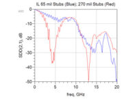
We worry about via stubs in high-speed designs because they cause unwanted resonant frequency nulls which appear in the insertion loss plot (IL) of the channel. But are all via stubs bad? Well, as with most answers relating to signal integrity, “It depends.”


Read More
Cover image

A Practical Method to Model Effective Permittivity and Phase Delay Due to Conductor Surface Roughness

Presented at DesignCon 2017

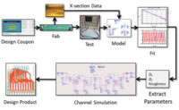
In the GB/s regime, accurate modeling of conductor loss and phase delay is a precursor to successful high-speed serial link designs. In this paper, a practical method to model effective permittivity and phase delay, due to conductor surface roughness, is presented. By obtaining the dielectric and roughness parameters, solely from manufacturers’ data sheets, phase delay and effective permittivity can now be easily predicted. Detailed case studies and several examples test the model`s accuracy.


Read More
Fig 4

Controlling Electromagnetic Emissions from PCB Edges in Backplanes

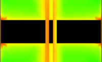
It is a well-known fact that electromagnetic radiation can be emitted from the edges of printed circuit boards (PCBs). When a current carrying via passes through two or more reference planes, an EM wave propagates radially away from the via within the cavity.  It is guided by the respective planes; much like a water ripple will propagate radially away from a rain drop hitting a puddle of water. When the wave meets the PCB edge, the two reference planes form a slot antenna and will radiate noise with the potential to generate electromagnetic interference (EMI) to nearby equipment.


Read More
Eye Diagram

Practical Method for Modeling Conductor Surface Roughness Using Close Packing of Equal Spheres

Presented at DesignCon 2015

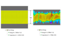
In the GB/s regime, accurate modeling of conductor losses is a precursor to successful high-speed serial link designs. In this paper, a practical method for modeling conductor surface roughness is presented. Obtaining the roughness parameters solely from manufacturers’ data sheets, conductor loss can now be accurately predicted from first principles. By using a close packing of equal spheres model, the radius of the spheres and area of the multi-sphere tiled base are determined then applied to the Huray “snowball” model. A case study, based on Megtron-6 and N4000-13EP dielectric with HVLP and VLP copper foils respectively, validates the model’s accuracy.


Read More
View All Articles by Bert Simonovich