

This extreme measurement seems more impossible than difficult. The traditional stability assessment method for voltage regulators is the Bode plot. Access to the control loop is required and a small signal is injected into the control loop, usually through a resistor, placed at the top of the voltage sense divider, for this purpose as shown in Figure 1.

Figure 1 Signal injection locations for the Bode plot measurement of a voltage regulator. The example shown here is used to indicate that most modern voltage regulators include multiple control loops, and in the best case, only one is accessible.
Without access to this voltage divider, there isn’t a place to inject a signal into the control loop, and therefore the Bode plot is seemingly impossible.
One option is to use an alternate assessment method, such as non-invasive stability measurement (NISM), shown in Figure 2. This alternate solution provides the effective phase margin as 64.39 degrees. While this solution does provide the phase margin, the request wasn’t for the phase margin, but for the Bode plot, requiring a bit more work.

Figure 2 An alternate method such as NISM can be used to assess the stability; however, the result is not the requested Bode plot.
Going back to small signal theory, a relationship between Open Loop, Closed Loop and the loop gain vector, T was presented as

Solving for the loop gain vector T

The output impedance plots, shown in Figure 2, represent both the Open Loop (with power off) and Closed Loop (with power on) impedance.
Having both the ON and OFF state plots allows us to compute the Bode plot from this data, as shown in Figure 3.

Figure 3 The Bode plot is mathematically derived from the OFF and ON impedance measurements, representing the Open Loop and Closed Loop functions.
The result in Figure 3 is in excellent agreement with the result in Figure 2, but now the data is provided as a Bode plot, as requested.
A few tips for using this method. Measure the impedance as close as possible to the sense point, which is often internal to the voltage regulator, so at the pins. Also, ceramic capacitors have significant DC Bias effect, so if the capacitors are ceramic, the OFF state should be measured at the operating voltage using an external bias source.
As is often the case, this accomplishment results in a request for something yet more difficult. In this case, the request is to obtain the Bode plot for a switching regulator in a typical AC adapter, but without removing the PCB from the housing and with a short cable accessible, outside the housing, for the measurement. As a reminder, the measurement needs to be performed close to the voltage sense divider, which is inside the housing and so inaccessible for the measurement.
While the measurement cannot be performed inside the housing, at the other end of the cable we can use another method to obtain the same result.
Using a TDR at the end of the cable, the cable is measured and reflected as a series resistance and inductance (Figure 4). Mathematically subtracting this resistance and inductance directly, or using a de-embedding block in a simulator, the ON and OFF measurements from the end of the cable are re-referenced to the output capacitor inside the housing.

Figure 4 Using a TDR to create a simple model of the cable, the cable is mathematically subtracted or simulated using a simulator de-embed block to move the measurement to the internal output capacitor.
Applying the same small signal transformation applied for Figure 3 provides the Bode plot, as it would appear inside the housing, as shown in Figure 5.
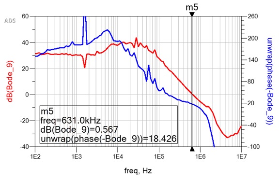
Figure 5 After mathematically removing the cable from both ON and OFF measurements performed at the end of the cable, the measurements are re-referenced to the internal output capacitor. The small signal transformation is used to transform the ON and OFF impedance measurements to the loop gain vector T, plotted as dB magnitude and Phase, aka a Bode plot.
This example was originally presented at DesignCon 2021.