
The 2-port shunt through measurement is an adaptation of 4 wire Kelvin measurement system using a vector network analyzer (VNA) for measuring very low impedances, in the order of milli/micro ohms. The method is becoming popular due to its importance in measuring power distribution network (PDN) impedance. In this paper, we show the theory behind 2-port shunt through measurement using VNA and how the inherent ground loop introduces measurement error. Finally, we propose solutions for the ground loop problem with measurement results. This paper won an Outstanding Paper Award at EDI CON USA 2018.
The 2-port shunt through measurement is the gold standard for measuring milli-ohm impedance while supporting measurements at very high frequency. These capabilities make it ideal for measuring a power distribution network (PDN). This paper shows how to make a 2-port shunt through measurement using a commercial vector network analyzer (VNA). Unfortunately, this measurement includes an undesirable ground loop. Left uncorrected, the ground loop introduces significant errors.

Figure 1. 2-port shunt through impedance measurement setup using a commercial VNA Omicron Bode 100 to measure low impedances
(ZDUT << 50Ω).
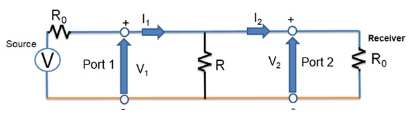
Figure 2. Equivalent circuit diagram of 2-port shunt through measurement shown in (Figure 1)
to measure R.
Figure 1 shows the conventional 2-port shunt through measurement set up. Figure 2 shows the circuit configuration to measure a small valued resistor in 2-port shunt through measurement. From the definition of S21 [1, pp. 2-3],

Solving for R we get,

where it is assumed that R0 = 50 Ω and S21 << 1 (True for very small impedance magnitudes/resistances - R << R0). Equation 1 is less intuitive in 2-port shunt through measurements. Another representation of the definition of S21 is shown in [1, pp. 2],

Equation 3 results in same value for S21 upon simplification. The difference here is that this gives an intuitive feeling for what is happening with S21. The denominator is constant for a VNA, if the source and receiver impedances are fixed. One exception to this is proposed by Steve Sandler in his paper “Extending the usable range of the 2-port shunt through impedance measurement” [2]. Here the source R0 is increased to shift the measurement window. Source R0 is increased to a higher value by adding an external resistor say, 450 Ω and the Rs now becomes 500 Ω for a 50 Ω VNA assuming that the frequency range we are interested is such that the external resistor is electrically very small and is a lumped element at that frequency. What we do here is that we reduced the maximum power that can be sourced from a VNA, which increases the range of impedances that can be measured. It should be noted that the sensitivity is an inherent property of a VNA and is not changed.
In Equation 3, S212 is the received power in Rx, scaled by the power that would have been received, if the DUT was not present. Let us look the effect of this in 2-port impedance measurements. R = 25S21, and S21 increases when the received power increases.
Any increase in the received power will be reflected as an increase in the measurement of R.
Non-idealities
Like all measurements, the 2-port shunt through measurements suffers from non-idealities. Figure 3 shows two non-idealities,
- Cable losses
- Ground loop

Figure 3. Non-idealities added in the 2-port shunt through measurements
Every cable will have cable losses that are marked as cable resistances in Figure 3. All grounds in a VNA are connected together at the front panel RF ground. This results in a ground loop in the 2-port shunt through measurements as shown in Figure 3.
Ground loop problem

Figure 4. Common mode current formation due to the ground loop
Figure 4 shows an alternate path for signal current return seen as common mode current. The addition of ground connections created this path. If this path never existed, all the current would have returned through the cable. The new path created an additional path for current which depends upon the value of RG. In almost all VNAs, RG << Rcable1b and Rcable2b. So, the additional current will be much larger compared to the case of not having this additional path. This additional current adds more power in the receiver which causes an increase to S21 and, in turn, the estimated R which 25S21. This is an error in measurements, and does not relate to the actual value of R. So, this will be treated as an error.
Example

Figure 5. Example to estimate the ground loop error
Let us take an example to estimate how much error results from common mode current created by the ground loop. Figure 5 shows an example where the two cases of having and not having a ground loop is studied. A small resistance (RG = 10-15 Ω) is placed in the loop to mimic the ground loop connection and a large resistance (RG = 1015 Ω) is placed in the loop to mimic the ground loop connection. The circuit can be solved with any SPICE program to estimate the power consumed by the receiver in these two cases,
- RG = 10-15 Ω
- RG = 1015 Ω
We can use Equation 3 to estimate the S21. The denominator, Power absorbed by Rx when DUT is absent = 5 mW (cable losses are neglected and is assumed that no port extension through calibration) is the maximum power that can be transferred from the source. This is a constant with respect to a VNA. The S21 for these two cases are,
- S21 =
 = 0.022538
 - S21 =
 = 0.0036841
As we expected in case 1, there is more power consumed by the receiver due to the higher common mode current. The estimated R from S21 based on R = 25S21 are,
- S21 = 0.56344
- S21 = 0.092101
The error due to ground loop is nearly 460 %. The small deviation in case 2 comes from our approximations and assumptions. The example was done for DC. The same approach can be performed for an AC case too. This is left to the interested readers.
It is clear from this example that we need to minimize the common mode current which contributes large error in 2-port shunt through measurements.
Ways to Address Ground Loop Problem

Figure 6. Removing ground loop in 2-port shunt through impedance measurement setup shown in Figure 1.
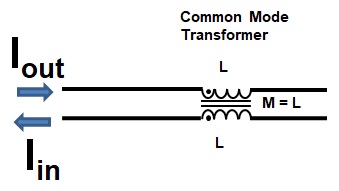
Figure 7. Common mode transformer circuit
Figure 6 shows a solution to the ground loop problem. The obvious way to minimize the measurement error is by minimizing the common mode current. We have developed has two produts to minimize common mode current
Figure 10 shows the experimental results using the Picotest common mode choke (J2102A) and semi-floating differential amplifier (J2113A).
The first approach is to introduce a high quality 50Ω common mode transformer or common mode choke. As the name indicates, it blocks common mode current. Figure 7 shows the equivalent circuit of a common mode transformer. The common mode transformer is built on a ferrite core such that when Iout = Iin, the inductance offered to the current flow is zero. The part of this current is called the differential current. This is the current that contributes to the normal operation.
When a part of the current flows through one but does not return through the other, it is called common mode current. The common mode transformer shows a very large inductance to this current flow and effectively blocks this. The amount of blocking (attenuation) highly depends upon the design of the transformer. Since this transformer should not affect normal VNA measurement operation, it has to be designed such that the impedance seen by the differential current is 50Ω. An important consideration is that the common mode choke is not effective at DC or low frequency. The maximum frequency at which the common mode transformer is effective depends upon the core and is determined by the quality of the material. We found better measurement results when the common mode choke is connected in the receiver loop as shown in Figure 8.

Figure 8. Common mode transformer included in two-port shunt through measurement circuit

Figure 9. Semi-floating differential amplifier included in two-port shunt through measurement circuit
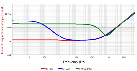
Figure 10. Comparisons of methods for ground loop problem in 2-port shunt through impedance measurements while measuring
a 1mΩ resistance
Another approach to the ground loop problem is to use a semi-floating differential amplifier, which shows large resistance to common mode current. Because it is resistance, the semi-floating amplifier is effective at DC too. Better measurement results are observed when it is connected in receiver loop as shown in Figure 9.
Conclusion
The two-port shunt through is an important measurement method to measure very low impedances. As the PDN impedances that need to be measured are decreasing based on the higher chip functionality requirements, the method is gaining popularity. Currently, the commonly designed PDN target impedance is in the milli-ohm range. However, some of the advanced PDN designs are in the range of micro ohm. This makes the two-port shunt through measurement an important method for PDN designs.
Unfortunately, the 2-port shunt through measurement topology has an inherent ground loop. One way to address this problem is by breaking the ground loop. Two methods (common mode choke or semi-floating differential amplifier) to break ground loop are proposed in this paper. The common mode choke is not effective at DC while a semi-floating differential amplifier is an effective solution even at DC. Measurement results for both these proposed solutions were presented to show the effectiveness of these methods. Accurate PDN measurements require ground loop isolation with flat frequency characteristics and uniform 50 W impedance. General purpose or homemade solutions may not provide the flat, 50Ohm impedance required. As a result, it is important to verify your isolator or use one made specifically for this purpose.
Note that one way to help reduce the impact of the ground loop is to minimize the resistance in the ground connections from the VNA to the DUT.
References
[1] R. W. Anderson, “S-parameter techniques for faster, more accurate network design,” HP application note 95-1, Feb. 1967.
[2] S. M. Sandler, “Extending the usable range of the 2-port shunt through impedance measurement,” IEEE MTT-S Lat. Am. Microw. Conf. (LAMC), pp. 1–3, Dec 2016.
[3] J. Y. Choi and I. Novak, “Simulating and Measuring Microohms in PDNs”, DesignCon 2015
Author(s) Biography
Anto K Davis received a B.Tech. degree in Electrical and Electronics Engineering from the National Institute of Technology Trichy, India, in 2006, as well as M.Tech. and Ph.D. degrees in Electronics Design from the Indian Institute of Science, Bangalore, India, in 2010 and 2015 respectively. He was employed by Huawei Technologies, Bangalore, India, from 2006 - 2007, and by Brocade Communications, Bangalore, India, in 2011. He served as a postdoctoral researcher at the School of Electrical and Computer Engineering, Georgia Institute of Technology, Atlanta, USA, from January 2016 to December 2017. He is currently working as a Senior Technology Strategist at Picotest in Bangalore, India (started in January 2018).
His Ph.D. research addressed noise reduction techniques for microprocessor - power distribution networks (PDN), and methods to suppress anti-resonance peaks. Currently, he is investigating stability of switching and linear converters at Picotest. His research interests include: electromagnetic compatibility, power integrity, stability analysis of switching power converters, control of power converters, switched capacitor converters, switched inductor converters, wireless power transfer, and internet of things.
Steven M Sandler has been involved with power system engineering for nearly 40 years. The founder and CEO of Picotest.com, a company specializing in instruments and accessories for high-performance power system and distributed system testing, Steve is also the founder of AEi Systems, a company that specializes in worst-case circuit analysis for high-reliability industries.
He frequently lectures and publishes internationally on the topics of power integrity and distributed power system design. His most recent books include: Switched-Mode Power Supply Simulation with SPICE (2018) and Power Integrity: Measuring, Optimizing and Troubleshooting Power-Related Parameters in Electronics Systems (2014). Steve is a winner of the Jim Williams ACE Award for Contributor of the Year (2015) and the recipient of both the DesignCon 2017 and EDICON USA 2017 Best Paper Awards.