
With the growth of 5G data traffic and AI computing, data centers need faster connectivity to meet the increasing bandwidth. High speed I/O speed beyond 112 Gb/s per lane is required. If we follow the SerDes technology revolution by doubling the data rate per lane in every 2-3 years, the next generation I/O data rate will be 224 Gb/s. This article explores options, technical challenges, and potential solutions to achieve 224 Gb/s per lane.
Options to achieve 224 Gb/s per lane
To achieve 224 Gb/s per lane, the leading options for consideration are:
- Double the signaling rate:
The current 112 Gb/s per lane electrical interfaces predominantly use the 4-level pulse-amplitude modulation (PAM4) modulation scheme at a baud rate of 56 Gbaud, 4-level signaling with 2 bits per symbol. If we stay with PAM4 modulation, the data rate of 224 Gb/s requires a baud rate of 112 Gbaud.
- Increase the constellation size:
To totally avoid increasing the signaling rate for 224 Gb/s compared with 112 Gb/s PAM4, a higher level modulation scheme such as PAM16, 16-level signaling with 4 bits per symbol, would be needed. Alternatively, PAM6 and PAM8 can achieve 224 Gb/s by increasing the signaling rate to 86.7 Gbaud and 74.7 Gbaud respectively.
- Use fiber-optic cables:
With signaling rate increasing, electrical channels like PCB traces or copper cable both have bandwidth limitations over certain reach distances. Alternatively, optical fiber cables can be used to transmit high bandwidth data over long distances. There are new emerging technologies such as chiplet and co-packaging optics (CPO) where the majority of the channel is in the optical domain.
Challenges and Potential Solutions for 224 Gb/s SerDes
For the Option 1 to double the signaling rate, the major challenges are:
- Can the channels (PCB traces, connectors and cables) support the 2x bandwidth?
- Can the SerDes design practically meet the 2x sampling rate and bandwidth?
Figure 1 shows two 112G chip-to-module reference channels. Chip-to-module 2 (right) has a roll off before 56 GHz (the Nyquist frequency of 224 Gb/s PAM4 modulation) while chip-to-module 1 (left) pushes the roll off beyond 60 GHz. From the channel frequency responses, we could expect chip-to-module 2 is more difficult to drive 224 Gb/s PAM4 signals through than chip-to-module 1 due to its bandwidth limitation. Besides channels, SerDes devices have to double the analog front-end bandwidth and sampling rate to operate at 112 Gbaud. Moore’s Law predicts that circuits are able reach the speed, but the real challenge is the trade-off between performance, power, and cost.

The challenges for the Option 2 to increase constellation size are:
- Signal-to-noise ratio (SNR) penalty for higher modulation levels
- Higher complexity for SerDes design
- Higher sensitivity to noise and jitter
Table 1 lists key parameters for different PAM schemes, such as the number of bits per symbol, signaling rate, unit interval, fundamental frequency, SNR penalty, and jitter tolerance. We can see that increasing modulation levels can help reduce the bandwidth and the sampling rate, but with the cost of higher SNR penalty and sensitivity to noise and jitter.

For Option 3 (using optical cables instead of PCB traces or copper cables), we can study the next-generation application spaces shown in Figure 2. With signaling rates increasing, electrical channels might reach capacity and have to shorten the distance. PAM4 signaling can drive die-to-die/OE, chip-to module, chip-to-chip, and even chassis-to-chassis interfaces through substrate traces within a package, PCB traces over a board, or copper cables at 112 Gb/s. Can these 112 Gb/s electrical channels still support 224 Gb/s?
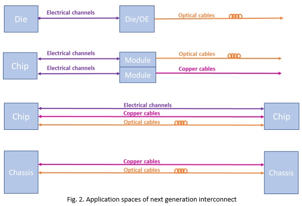
An example set of reference electrical channels for 112Gb/s [1] for die-to-die/OE (d2d), chip-to-module (c2m), chip-to-chip (c2c), and chassis-to-chassis through direct attach cable (DAC) are selected for this study of 224 Gb/s suitability. Table 2 shows their insertion loss (IL), figure of merit insertion loss deviation (FOM_ILD) and integrated crosstalk noise (ICN) with different PAM modulation levels PAM4, PAM6, PAM8, and PAM16.

We can see that the higher level modulations offer bandwidth reductions such that channel IL, FOM_ILD, and ICN impact less. However, higher modulation levels require higher slicer SNR to achieve a certain detector error rate (DER). For example, the required SNR at the SerDes slicer to achieve 1e-6 DER are 13.54 dB, 20.67 dB, and 26.96 dB for NRZ, PAM4, and PAM8 modulation schemes, respectively. The trade-off between spectral benefit and SNR penalty make the modulation scheme selection more complicated, requiring detailed analysis.
To study the performance trade-off for different modulation schemes, the method of Salz SNR for an ideal decision feedback equalization (DFE) receiver [2] with added implementation penalties is used. Figure 3 shows the block diagram of a link model and Table 3 gives the modeled impairments and their values included in the simulations.


- Die-to-die/OE channel capacity supports PAM4 signaling at 224 Gb/s
- PAM4 and PAM5 modulation schemes are good for chip-to-module channels
- PAM5 and PAM6 modulation schemes outperform PAM4 when channel loss increases
- Longer channels such as chip-to-chip or DAC applications require stronger FEC [3] than shorter channels to relax DER target but with the cost of encoder/decoder latency and complexity


Summary
From the channel capacity and SNR margin, we can conclude that electrical channels will continue to be viable after 112 Gbps. For longer distances, such as chip-to-chip and chassis-to-chassis interfaces, higher modulation schemes (PAM5 or PAM6) can be used to relax channel bandwidth requirements. Promising results for die-to-die/OE and chip-to-module analysis should enable co-packaging and pluggable optics at the next speed node.
Reference
[1] IEEE P802.3ck Task Force – Tools and Channels: http://www.ieee802.org/3/ck/public/tools/index.html
[2] J. Cioffi, and et. al., “MMSE Decision-Feedback Equalizers and Coding-Part I: Equalization Results,” IEEE trans. On Comm., Vol. 43, No. 10, October 1995.
[3] Cathy Liu, “What is FEC, and How Do I Use It?” Signal Integrity Journal, https://www.signalintegrityjournal.com/articles/1284-what-is-fec-and-how-do-i-use-it
Bio
Cathy Liu, Distinguished engineer and SerDes architect in Broadcom