
Data converter based SerDes designs are gaining popularity due to their flexibility in architecture and powerful digital signal processing (DSP) equalization. For the first-generation ADC based RX, most of the attention has been focused on implementation of high-speed and high-performance ADCs due to their various challenges. Very little systematic analysis and study has been published regarding the optimal location of equalizers (like feed forward equalization; FFE) to achieve the best system performance.
Conventionally, in a mixed signal SerDes, the FFE is placed on the TX side thanks to its simpler implementation of delays and gains. Typically, TX side FFE, a.k.a., TX FIR, is limited to 3 to 5 taps. However, TX FFE suffers from the peak power constraint, which in effect attenuates the average power of the outgoing signal. As the data rate increases beyond 25Gbps, the pre-cursor intersymbol interference (ISI) in a backplane/copper cable system becomes non-negligible. Thus, the need for a power-efficient FFE is ever more important to effectively deal with pre-cursor ISI as well as long tails in the channel pulse response. (Basically, TX FFE follows L1-norm coefficient normalization.)
On the other hand, a RX FFE does not require L1-norm coefficient normalization and does not come with the same peak power constraint as TX FFE. Even though the analog RX FFE might be subject to other coefficient constraints due to nonlinearity requirements, the front-end noise is amplified by the L2-norm of FFE coefficients. Furthermore, the digital RX FFE coefficients can be more easily and optimally adapted to achieve the best tradeoff between cancelling the channel ISI and mitigating the amplification of system noise. However, a true analog FFE that covers a wide range of data rates is difficult to build for reasonable power and nonlinearity.
The emergence of ADC-based RX allows system and circuit designers to re-evaluate the choice of TX FFE vs. RX FFE. This paper offers theoretical analysis, realistic simulations and practical comparisons between TX and RX FFE. The FFEs are adapted using the least mean square (LMS) algorithm for all the examples. For simplicity, no DFE is included in the system. However, since the DFE typically is the last equalizer in the link and it does not boost crosstalk or noise, the comparison is fair and the conclusions should provide important insights to the industry that is currently facing challenges at 56G and soon to be facing them at 112G.
In addition, the effects of TX DAC and RX ADC quantization will also be studied. The nature of quantization error is discussed and further incorporated into the existing analysis framework. Behavioral simulations with varying noise, quantization, and FFE settings are performed to verify insights and draw conclusions. For some long-reach copper channels intended for 112G applications, a tradeoff simulation is performed to find the best solution space with varying number of FFE taps and converter resolutions.
Finally, we present DAC and ADC silicon implementation challenges. At such demanding speed, clocking becomes a crucial aspect, and the line between digital and analog circuits becomes blurry. State-of-the-art work is surveyed to provide better comparisons and demonstrate feasibilities.
SNR Analysis between Two Locations of FFE
Study of FFE location has been gaining more attention. Work of [1] proposes a long TX FIR that results in a simpler receiver and more power efficient link. As shown in Figure 1(a), the authors of [1] suggest that moving the receiver FFE to the transmitter side would decrease the RX FFE power due to digital multiplications.

System simulations show the performance differences between the two schemes in Figure 1(b) and 1(c). The TX FFE scheme is shown to have larger eye opening, thus better system performance. As highlighted in Figure 1(b), the main disadvantage of the RX FFE according to [1] is the implementation cost when many far-out taps with small coefficients are needed to cancel residual ISI due to impedance discontinuities and reflections.
However, what is not clear in [1] is that some FFE is present on the receiver side that shapes the channel further along with the continuous-time linear equalizer (CTLE). The authors actually propose only to move the far-end long tail taps of the FFE to the TX side in order to handle reflections. This fact prompted our thinking that RX FFE and a more analytical and systematic study is still necessary.
Recent works, such as [2], have shown system level feasibility of PAM4 link architectures for long reach applications at 112G. With reasonable assumptions of SerDes architecture and realistic noise and jitter sources, the authors concluded in [2] that RX FFE could deliver much better performance in terms of eye opening (eye height and eye width) than the performance when the FFE is placed on the TX side. This is summarized in Figure 2.

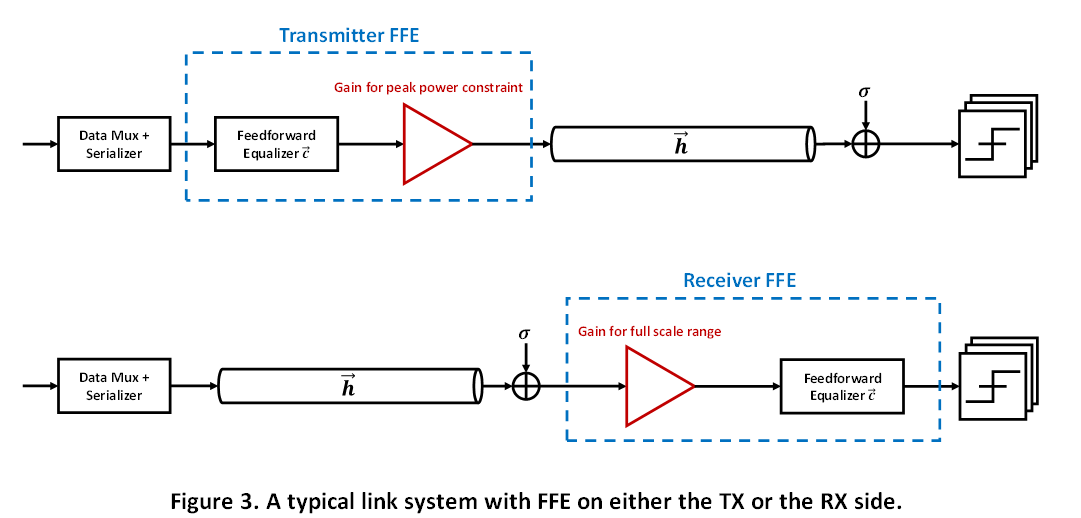
However, there was no detailed explanation for this phenomenon in [2]. Therefore, in this paper we provide in-depth analysis based on link performance margin in terms of signal to noise ratio (SNR) and theoretical explanations to the mystery of FFE locations. In this section, a theoretical framework is developed first to understand effects of the FFE’s location in a typical link system. SNR will be used as the metric for comparing the performance. Figure 3 shows a simplified block diagram of typical link systems with FFE either on the TX or the RX side. The SNR comparison point is chosen at the input of decision feedback equalizer (DFE) because it is common to both architectures. We investigate system performance with FFE as the only means of equalization. We assume ideal timing and clock recovery to restrict the scope of analysis, which allows system simulations and evaluations in the discrete time (DT) domain.
Theoretical Analysis of System SNR
The nonidealities considered in this analysis are ISI, modeled by the pulse responses, and an independent identically distributed (i.i.d.) Gaussian noise at the RX input. Sources of input noise include thermal noise of termination, input-referred RX circuit noise, and crosstalk from neighboring aggressors.
Conventionally, the FFE is on the TX side because it does not boost noise and more importantly has a simpler implementation. However, TX FFE coefficients must be normalized due to a maximum output swing limited by power supply, also known as peak power constraint. Thus, for an equalizer with P pre-cursors and Q post-cursors, the transmitted signal amplitude is directly attenuated by a normalization factor of  the L1-norm of the equalizer coefficients
For the purpose of this analysis, we enforce the main cursor tap of FFE to be 1, i.e.,  The resulting SNR for TX FFE system is given by Equation (1), in which
  is the channel (bump to bump) pulse response.
  is the main cursor of the equalized channel divided by the number of eyes given a modulation M (e.g., for PAM4, M=4 and there are M-1=3 eyes). a is the signal RMS strength given a modulation (e.g., for PAM4, a = 0.745 ).
  are standard deviations of residual ISI and RX input noise, respectively.
The same analysis can be applied to the system with FFE on the RX side. The FFE will equalize the channel in the same fashion (assuming the same coefficients as the TX FFE for now), but boost the RX input noise power. Specifically, the input noise power is amplified by the L2-norm  of the FFE coefficients,
  The corresponding system SNR is shown in Equation (2).

Using these two SNR expressions, an immediate comparison can be drawn. Assuming enough FFE taps are used and residual ISI at the decision-making point is not the dominant noise source in the system, the SNRs above simplify to Equations (3) and (4), respectively.

It becomes apparent that the SNRs of the architectures of interest only differ in the extra attenuation due to either FFE coefficients L1 or L2 norm. It is well known that for any given vector  therefore the system performance with RX FFE is at least as good as that with TX FEE as shown in Equation (5)

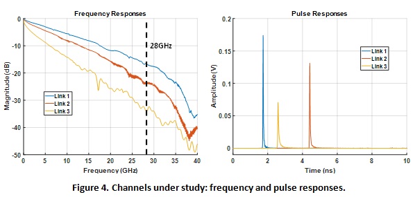
To validate the inequality in Equation (5), we consider three different channels used for 112Gbps PAM4 applications as shown in Figure 4. The channel losses at 28GHz (the Nyquist frequency) are approximately 16dB, 24dB, and 33dB, respectively. The same FFE coefficients are applied to both the TX and RX FFE, and they are calculated to cancel ISI at sampling phase of interest completely (zero forcing), given the number of pre- and post-cursor taps. The following describes the steps to calculate SNRs for a given channel and selected number of pre-cursor and post-cursor taps:
- Compute the zero forcing FFE coefficients.
- Convolve the computed equalizer coefficients with DT channel pulse response to obtain the equalized pulse response.
- Calculate residual ISI noise power and multiply it by a .
- Find the L1 and L2 norm of the FFE coefficients.
- Use Equation (1) and (2) to calculate SNRs for system with TX or RX FFE.
RX input noise strengths is swept from 0mV to 5mV rms. The maximum TX swing is held at  400mV. The FFE lengths used for this analysis are a) 5 pre-cursor + 15 post-cursor taps, b) 10 pre-cursor + 20 post-cursor taps, and c) 15 pre-cursor + 25 post-cursor taps. Figure 5 shows the calculated system SNR with respect to input noise amount for all three channels and FFE lengths considered.
For any channel and FFE length, we see the obtained RX FFE system performs as well as the TX FFE system. Due to the linear nature of the systems under study, FFE has the same effect on the system regardless its location when there is no RX input noise  However, a large discrepancy manifests itself when RX input noise is considered. TX FFE performances roll off much faster than that of the RX FFE. The system SNR difference can be more than 6dB when
  is larger than 2mV for the worst-case channel when comparing TX and RX FFEs.
For channels with larger losses (link 2 and link 3), increasing the FFE lengths improves performance noticeably. However, there is no significant difference between the 30-tap and 40-tap settings. Link 3 is a particularly difficult channel to operate in the presence of RX input thermal noise. As a result, TX FFE can hardly equalize link 3.
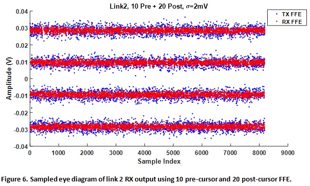
We ran behavioral transient simulations to verify the system SNR equations. A PRBS13 data pattern is used for simulation time and enough data length to capture most of ISI. Figure 6 shows an example of sampled eye diagrams for both TX and RX FFE systems. We can visually conclude that RX FFE has a much higher system SNR given the error spread around the data levels. The exact SNR value is calculated by finding the ratio of eye opening and error spread. Errors are found by subtracting the output value with the ideal data levels.
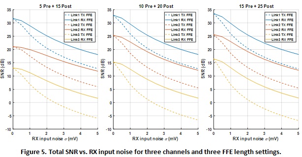
Figure 7 shows the system SNRs from the behavioral simulations plotted with the previous analytical results. The transient simulation results almost overlap with the analytical curves, proving the validity of the analysis. Once we are confident about the analysis framework, we are able to add more non-idealities in later sections. Adaptive equalizer performances can also be demonstrated with behavioral simulations.

Equalizer Adaptation
Another motivation for putting the FFE on the RX side is the equalizer adaptation capability. When adapting FFE on the TX side, a back channel is required, which leads to further complexity and overhead. This becomes even more challenging for different vendors of silicon to interoperate. On the other hand, RX side FFE can provide more robust system performance due to its true nature of adapting the coefficients to the system variations due to PVT.
Conventional FFE adaptation uses the LMS algorithm, which is a steepest gradient descent algorithm that aims for the minimum mean square error (MMSE) solution. Another advantage of RX adaptation is its ability to find the optimal tradeoff among different noise sources. Furthermore, it is more realistic to discuss situations in which TX FFE does not operate with the optimal FFE coefficients due to lack of adaptation. To capture this effect, 5% random errors are added to the ZF FFE coefficients. This translates to extra residual ISI that significantly degrades the system performance.
Figure 8 shows the simulation block diagram to compare performance between ZF TX FFE, ZF RX FFE, and MMSE RX FFE. To visualize plots and discuss results more effectively, only link 2 (moderate loss) is considered, since the observed trends should be the same for the other channels. Figure 9 shows the SNR results against input noise power. It is clear that adaptive RX FFE outperforms ZF TX FFE with coefficient offsets.

In this particular case, we have purposely shown a 30-tap setting with random error added that has worse performance than another 20-tap setting for ZF FFE. This is due to the resultant erroneous 30-tap coefficients not canceling channel ISI as effectively as the randomly generated 20-tap coefficients. For the RX adaptive FFE, the system is still able to show improvements with more taps and has significant advantage over the ZF FFEs. Having the adaptation capability on the RX side in order to track any operating environment and circuit variations is important not only for nominal system performance, but also for robustness under various conditions.

DAC and ADC Resolution Practical Considerations
In this section, we include more realistic system building blocks, such as DACs and ADCs, to understand their effects and limits in the context of FFE equalization and system performance. When a large number of FFE taps are needed, digital equalizers are the better option because mixed-signal implementations of FFEs become heavily limited by the circuits’ own parasitics (see Section 4). Therefore, data converters are necessary to make the transition between analog and digital signal processing.
A DAC is used on the transmitter side to convert a digital equalizer output into an analog signal that is driven onto the channel. An ADC is used on the receiver end to convert the channel output signal into digital codes that will be further processed by the subsequent DSP. For our theoretical analysis, we will assume that the FFE coefficients have much higher resolution than that of the converters. In other words, we want to focus on the limits of the converters and their impact on system performance. Behavioral simulation results are presented and conclusions are drawn, specifically regarding the effectiveness of FFE in the presence of the converters, as well as the tradeoff between FFE lengths and converter resolution.
DSP-based Serial Link System Architecture and Modeling
Figure 10 shows the modified block diagram of the system of interest. A DAC is added after the TX FFE and an ADC is placed before the RX FFE.

There is intrinsically a quantizer in front of the DAC to limit the output resolution of the FFE. ADCs naturally acts as quantizers themselves. Thus, both architectures include quantizers that bin multiple input values into the same output value. One of the most important non-idealities of quantizers is finite resolution, which is our analysis focus for simplicity.
In the case of infinite resolution FFE coefficients, the quantizers in both architectures can have the same staircase shaped DC transfer function as shown in Figure 11. The converters’ resolution (specified by number of bits) determines the number of levels and step size in the transfer curve. In the example plots, a 3-bit converter is used to exaggerate the staircases for clarity. A quantization error plot can be obtained by subtracting the quantized output from the ideal input. A saw tooth curve (middle plot) shows a ½ step-size bound. We can also plot the histogram of the quantization errors when a random input is applied. Due to data converters’ intrinsic quantization errors added to the system, bit error ratio (BER) will increase.
