
Through the years there has been very little written about the current carrying capacity of a via. This is, I believe, because there has been no practical way to measure or to predict the temperature of a via. We have blindly assumed that it is the current through the via that determines the via temperature, and approached board designs accordingly. Board designers typically approach the question of via size using one of three strategies:
- Simply don’t allow vias that carry higher levels of current. Route all the conductors on a single trace layer.
- Size the via to handle the current using the IPC 2152 (Note 1) guidelines.
- Use a “standard” via known to be able to carry a certain amount of current and use multiple vias in parallel, as many as needed for the total current carried by the trace.
IPC 2152 explicitly endorses 2 and/or 3 on page 26:
The cross-sectional area of a via should have at least the same cross-sectional area as the conductor or be larger than the conductor coming into it. If the via has less cross-sectional area than the conductor, then multiple vias can be used to maintain the same cross-sectional area as the conductor.
Consider the thermal model (Notes 2 and 3) illustrated in Figure 1. It shows a pair of 76 mm (3.0 in) long, 0.69 mm (27 mil) wide, 1.5 Oz. traces (1.0 Oz. plating over a 0.5 Oz rolled copper trace) on either side of a board connected by a 0.26 mm (10 mil) diameter, 0.03 mm (approx. 1.0 Oz.) plated via. The via has about the same conducting cross-sectional area as the trace. The board is a few mm wider than the trace. The dielectric layer between the trace layers is 1.6 mm (63 mil) FR4. A thermocouple model (TC in Figure 1) is placed near the midpoint of the top trace. The purpose for this will be described later.

Figure 1
Thermal model of trace with via. (Not to scale)
If we assume for a moment that the trace is continuous with no via, and we apply 4.75 Amps of current to the trace, a simulation based on TRM results in a maximum trace temperature (not temperature change) of approximately 72.8 degrees C. If we model the board with the via, the simulation temperature at the thermocouple is still 72.8 degrees C while the temperature at the via is 70.1 degrees C (Notes 4 and 5).
So, now, here are three questions for you to ponder:
1. Why is the via temperature lower than the trace temperature?
2. If we apply 6.65 Amps to the model with a via, the trace temperature measured at the thermocouple TC will be about 114.2 degrees C. What will be the temperature at the midpoint of the via? Will it be higher, the same as, or lower than 114.2 degrees C., the temperature at TC?
3. If we widened the trace to 5.0 mm (200 mil), without changing the via, and applied more current, say 8.55 Amps, TRM simulation suggests the temperature at TC would be 44.8 degrees C. What would happen to the via temperature? (Note, 8.55 Amps would melt a 27 mil wide trace in less than 1.0 second!)
In the situations modeled here, with the current carrying cross-sectional areas of the trace and via approximately the same, the via temperature will be less than the trace temperature! The reason goes back to one of the surprising results reported in IPC 2152. Internal traces are cooler than equivalent external traces. This is so because the thermal conductivity of the board material is better than the thermal conductivity (convection) of the air. So vias cool more efficiently than do traces, and their temperatures are lower. A thermal profile of this simulation is shown in Figure 2. The maximum trace temperature is approximately half way between the pad and the via (at the thermocouple, TC).

Figure 2
Thermal profile of the top trace layer of the simulation at 4.75 Amps.
If we increase the current to 6.65 Amps (and the trace temperature increases to 114.2 degrees C), the via temperature will still be below the trace temperature. The simulation shows the via temperature will be 108.2 degrees C. It turns out via temperatures are always lower than trace temperatures with equivalent current-carrying cross-sectional areas.
So, what happens if we increase the trace width and the current, leaving the via exactly the same? The increased current works to increase the via temperature. But it turns out that the via temperature does not rise much above the trace temperature, whatever that is. The reason is the via length is very short compared to the trace width, and the trace becomes a strong heat sink for the via. So in this model, the trace temperature is 44.8 degrees C. while the via temperature is about 48.1 degrees C., about 3.3 degrees hotter than the trace temperature. This is hotter than the trace temperature, but not by a lot, especially considering that 8.55 Amps would melt a trace the same size as the via.
Conclusion
The inescapable conclusion from the above is that the conventional wisdom has been wrong! The current does not determine the temperature of the via, the associated traces do. As long as the traces are properly sized to handle the current, even a single, ordinary via is adequate to transition between trace layers. And the reason is because the thermal conductivity of the copper between the via and the trace provides a significant and effective heat sink for the via. The via simply can’t get a lot hotter than the trace.
This does not imply we should not be conservative when designing vias. It does suggest, however, that vias do not need to be as large as we thought nor does there need to be as many of them.
Empirical Verification
If there was ever a conclusion that cried out “SHOW ME!” this is it! Johannes and I knew we needed to build a real-world test board to confirm these results. Prototron Circuits (WA and AZ) graciously provided some test boards (Figure 3) (Note 6).
The relevant portion of a test board is shown in Figure 3. The board is approximately 60 mils thick FR4.The board contains 0.5 Oz. copper nominally plated with 1.0 Oz. additional copper. Two traces were compared, one nominally 27 mils wide, the other 200 mils wide. Each trace is 6.0” in length, one-half on the top layer and one-half on the bottom layer. There is a single 10 mil diameter plated via connecting top to bottom. The 10 mil diameter via plated to 1.0 Oz. has roughly the same conducting cross-sectional area as the 27 mil trace. It is important to note that the via structure is identical in each trace. The board was supported 2.5 inches above a plywood surface in still air by four screws at the corners. The board was microsectioned after testing to measure the actual dimensions for the simulation.
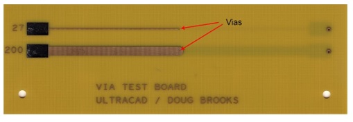
Figure 3
Relevant portion of via test board
We simulated the two traces, at two different currents each, and recorded the temperature results in Table 1. Then we applied the same currents to the traces and measured the temperatures with precision thermocouples. The actual temperatures are recorded in Table 2.
|
Result of Via Temperature Simulation |
||||
|
Trace width (mils) |
Current (A) |
Trace Temp. oC |
Via Temp. oC |
Via T/Trace T |
|
27 |
4.75 |
72.8 |
70.1 |
96.3 |
|
27 |
6.65 |
114.2 |
108.2 |
94.7 |
|
200 |
4.75 |
30.8 |
31.8 |
103.2 |
|
200 |
8.55 |
44.8 |
48.1 |
107.4 |
Table 1
Simulation results.
|
Measured Results of Via Tests |
||||
|
Trace width (mils) |
Current (A) |
Trace Temp. oC |
Via Temp. oC |
Via T/Trace T |
|
27 |
4.75 |
66 |
64.5 |
97.7 |
|
27 |
6.65 |
114 |
109 |
95.6 |
|
200 |
4.75 |
30.5 |
31.5 |
103.3 |
|
200 |
8.55 |
40.5 |
44.5 |
109.9 |
Table 2
Measured test results.
There are two especially important observations that should be made here:
1. First, a 6.6 Amp current through the 27 mil wide trace results in a via temperature of 109o C while a higher current of 8.6 Amps in a larger (200 mil wide) trace results in a much lower via temperature of only 44.5o C. This confirms that it is the trace that is controlling the via temperature.
2. The measured data (Table 2) are very close to the simulated data (Table 1). This gives us confidence that the simulation approach is a viable approach for predicting temperatures in complex situations.
Notes
1. IPC 2152, “Standard for Determining Current Carrying Capacity in Printed Board Design,” August, 2009, IPC, IPC.org
2. The results reported here come from Chapter 7 “Via Temperatures” in Brooks, Douglas G. and Adam, Johannes, “PCB Trace and Via Currents and Temperatures: The Complete Analysis. 2nd Ed.,” 2017, available at Amazon.com.
3. All thermal models in this article, and their solutions, will be based on the simulation tool TRM (Thermal Risk Management.) TRM was created by Dr. Johannes Adam, President of Adam Research (www.adam-research.com). TRM was originally conceived and designed to analyze temperatures across a circuit board, taking into consideration the complete trace layout with optional Joule heating as well as various components and their own contributions to heat generation. Learn more about TRM at http://www.adam-research.com.
4. The temperature at the thermocouple approximates the temperature of the trace whether or not there is a via present.
5. This temperature is higher than would be read from the IPC tables because in this simulation (1) the trace is shorter, (2) the board is smaller, and (3) the board material is different from that used in the IPC analyses. The via model needs to be smaller than the IPC boards for computational reasons. See Section 7.2, p 82, in Note 2 above.
6. The simulation model above is clearly based on this via test board. Earlier via studies led Johannes and me to the realization that we needed real-world boards to confirm the earlier results.