
Supply and ground bounce are the shifts in the supply and ground rails on the integrated circuit (IC) die with respect to their respective levels on the planes of the PCB. Any noise that is injected into the supply and ground path can appear at the logic inputs and outputs. It’s the edge rate that matters most, and this can cause EMI problems. Due to advances in CMOS technology and die shrinking, modern electronic device switching edge rates are much higher than previous technologies. In these types of ICs, the effects of intrinsic electrical characteristics become more pronounced.
One of these intrinsic electrical characteristics is the inductance found in all lead frame materials which creates the supply or ground bounce. Therefore, design strategies for reducing the ground bounce play an integral role in today’s higher speed embedded and digital systems. This article researches the ground bounce generated from an LCD display assembly while evaluating the impact of the ground bounce on the system level EMI. Three solution strategies to mitigate the ground bounce are analyzed, the pros and cons of each strategy are provided along with the test results.
Background on Ground Bounce
What is commonly referred to as supply and ground bounce is really the inductively coupled cross talk between I/O loop inductances. This inductively coupled cross talk is created when the wide data bus of an IC shares a common supply and return lead, which has parasitic inductance as shown in Figureure.1. Simultaneous switching noise (SSN) is often referred to as Vcc bounce or ground bounce [3].

Figure 1: Lead inductance of power and ground leads [4]
When the signal loop switches from logic 0 to logic 1, the current required to charge up must be drawn from the capacitance of the power subsystem. This current must pass through the parasitic inductance of the Vcc leads of the IC package. The package inductance prevents the current flow during these fast edge transitions. This voltage transient drives the supply (Vcc) rail of the IC negative with respect to the supply rail on the PCB and creates ringing on the DC supply rail [1].
Similarly, when the logic lines switch from logic 1 to logic 0, the parasitic capacitance of the transmission lines must be discharged through the parasitic inductance of the ground leads of the IC package. This di/dt acts as a forcing function and generates a voltage drop across the common return parasitic inductance. This voltage transient drives the ground of the IC positive with respect to the ground on the PCB and creates ringing on the ground plane [1].
These types of unwanted transients in the power and ground rail is the result of single ended logic drivers charging and discharging the on-die parasitic capacitors. Quiet outputs will move with the same waveform as the supply or ground bounce. These voltage transients can appear on all logic signals leaving the IC. So, it can appear on the Vcc rail, clock line, or data line leaving the IC. If a signal line has excessive supply or ground bounce, logic failures may result as well. These logic failures can be detected by the manufacturers during the prototype stage of the product. The EMI issues created by this unit may not be significant at the device level, but they can be severe at the system level. If the logic signal exits the faraday cage without a shield, it can cause EMI [1]. Connecting multiple points in a plane to “chassis ground” allows those currents to flow in the chassis, turning it into a radiating surface, worsening EMI. These issues are not clock related. In other words, low-speed PCB designs now have to deal with high-speed switching problems.
The Problem
As part of a development effort for one of our next-generation autonomous cleaning robots, we began doing EMC pre-compliance efforts. We had multiple EMI issues coming from our system. Further troubleshooting of the EMI problems led us to narrow the problem down to the touch-screen LCD display used in our robotic platforms.
The entire system is tested in an EMC chamber with a far-field antenna kept at 3 m distance from the system. In this case, the noise shown by Figure 2 is from an EMI scan of our entire robotic system with the LCD installed.

Figure 2 : 3-meter EMI Measurement Front Horizontal – Robotic system with LCD Display Rev A
The LCD display used in the robotic system was then tested separately, powered with an external power supply in a 3 m EMC chamber with a far-field antenna. The EMI measurement of the LCD display when powered by a 24 V external power supply is shown in Figure 3. It was verified that the 24 V power supply had no EMI noise prior to connecting it to the LCD display for additional EMI measurements. As shown by Figure 3, there is a significant amount of EMI in the system from ~200 MHz to 1 GHz (which was later verified to be created by the ground and supply bounce from the LCD display). It was then discovered that when this LCD unit is connected to a system with multiple PCBAs, the noise generated from the LCD conducted on to various cables which then radiated throughout the entire system.

Figure 3: 3-meter EMI measurement – Front Horizontal – LCD display Rev. A only
The LCD display assembly is composed of an LCD display unit and a driver PCBA. The LCD driver PCBA is using a STM32F429IIT microcontroller with a 176 pin LQFP package. The driver PCBA uses a 24 bit RGB bus to interface to the LCD display. Further investigation also revealed that the LCD driver PCBA provided only a few return paths on the microcontroller using this RGB data bus. The LCD driver PCB stackup analysis showed traces passing through the power and ground layers of the PCB. In order to find a correlation between the EMI and the source of the issue on the LCD display, further investigation was done on the power and ground rails of the LCD display assembly.
The supply and ground bounce created by the LCD unit was tested according to the test setup shown in Figure 4.

Figure 4: Test Setup used to Measure Supply (Vcc) and Ground Bounce [1]
The testing started with the Rev A version of the LCD PCBA. The measurements shown in Figures 6 through 8 were captured with a Tektronix MDO4054C oscilloscope connected to a low inductance probe as shown in Figure 5

Figure 5: Method to Measure the Ground Bounce with a Low Inductance Probe
Ringing was found on the supply (3.3 V) rail and output line as shown below (Figure 6). The peak-to-peak value of the ringing on the 3.3 V supply rail was 524 mV.

Figure. 6: CH1 (Yellow Signal) 3.3 V Vcc supply measured at pin 91 on STM32F4 IC on the LCD PCBA (with voltage offset removed), CH2 (Blue Signal) output line pin 3 (LTDC_B0)
Ringing was also discovered on the ground rail and output line as shown below (Figure 7). The peak-to-peak value of ringing on the ground rail was 748 mV.

Figure. 7: CH1 (Yellow Signal) GND measured at pin 90 on STM32F4 IC on the LCD PCB assembly, CH2 (Blue Signal) Output line pin 3 (LTDC_B0) - TTL signal
It was later realized that this ringing was being coupled to all the datalines as shown below in Figure 8.

Figure. 8: PIN 92 (CAN2_RX) with 700mV ringing
The spectral content of the EMI noise generated by these transient currents was beyond the capabilities of decoupling capacitors. If decoupling capacitors were added to such a system, the system would turn into a parallel resonant circuit making the ringing worse by creating oscillations during edge transitions [3]. The impact of the significant EMI issues created by the supply and ground bounce from the improperly designed LCD driver PCB forced an investigation for a proper solution to mitigate these issues.
Solution 1: Changing the stack up and adding plane capacitor
The EMI receiver response showed noise in the high frequency region (above 100 MHz). The controller PCB of the LCD unit was designed with a four layer stackup that included one internal plane as ground and one internal plane as +3.3 V (VDD). The plane pair was separated by 47+ mils of dielectric as shown in Figure 9. Both planes have signal traces embedded in them which compromised their integrity. We wanted to reduce the effect of high edge rates and poor PCB layout in our LCD display created EMI issues.

Figure 9: Layer stack up of the LCD driver PCB Rev A
In such cases, a plane capacitance in a PCB can reduce the EMI issues by filtering the noise at the PCB level. As per [1], the plane capacitance in a PCB is calculated (in farads) as shown by EQ(1).
 (1)
(1)
Where:
εo is the permittivity of free space, εr is the permittivity of the dielectric, A is the area of the PCB and d is the dielectric thickness used in the stack up
The original PCBA of the LCD unit uses ~47mils dielectric between the power and ground plane. This is not good enough to filter any of the high frequency EMI noise. So the LCD PCB was redesigned by adding more plane capacitors into the layer stack up as shown in Figure. 10. The dielectric thickness between the 3.3 V and Ground is reduced to 3mil. Another plane capacitor was added for the 5 V rail as some logic circuits in the driver PCBA also used 5 V. The power and ground planes were also designed without any traces passing through them. For all ICs in the design, power and ground nets connected directly to the respective planes ensuring the lowest line impedances possible.

Figure 10: Layer stack up of the LCD driver PCB Rev B

Figure 11: 3-meter EMI measurement – Front Horizontal – LCD display Rev. A vs. Rev B
The EMI receiver response for the new revision of PCBA, Rev B shows significant improvements compared to Rev A (Figure. 11). By adding plane capacitors to the PCB stackup, there is a ~10 dB to ~20 dB EMI noise reduction in the 200 MHz to 1GHz range, as shown in Figure 11. Unfortunately, it was realized after implementing the PDN filter solution that it would never be possible to mitigate all of the EMI noise created by the ground bounce from the LCD display. This is due to the fundamental limitation of the inherent inductance of the return paths within the microcontroller package available. This problem is package-related and it is very difficult to fix by actions taken on the PCB. The inductance in the ground lead is not the only inductance in the package; all of the output pins have an associated inductance. A better solution is to reduce the inductance in all leads. The design needs to be updated with a lower parasitic lead inductance package, such as a ball grid array (BGA).
Solution 2: Changing to a lower inductance microcontroller package
The next step was to investigate more about the packages and the typical parasitic inductances associated with each package. Typical parasitic lead inductances of a variety of IC packages are provided below in Table 1.
Table 1: Typical parasitic Lead Inductances of a Variety of IC Packages [5]
|
Package |
Typical Parasitic Lead Inductance |
Package |
Typical Parasitic Lead Inductance |
|
14 pin DIP |
3.2nH to 10.2nH |
14 pin SOIC |
2.6nH to 3.6nH |
|
20 pin DIP |
3.4nH to 13.7nH |
20 pin SOIC |
4.9nH to 8.5nH |
|
40 pin DIP |
4.4nH to 21.7nH |
|
|
|
40 pin TAB |
1.2nH to 2.5nH |
208 pin QFP |
5.31nH to 8.74nH |
|
44 pin QFP |
6.07nH to 7.06nH |
100 pin QFP |
6.69nH to 7.96nH |
|
20 pin PLCC |
3.5nH to 6.3nH |
119 pin PBGA |
0.15nH to 5.7nH |
|
28 pin PLCC |
3.7nH to 7.8nH |
249 pin PBGA |
0.13nH to 5.1nH |
|
44 pin PLCC |
4.3nH to 6.1nH |
624 pin CBGA |
0.5nH to 4.75nH |
|
68 pin PLCC |
5.3nH to 8.9nH |
456 pin PBGA |
0.2nH to 5.8nH |
Voltage across an inductor as a function of time is given by equation (2). In this case, the edge rate can be substituted for time.
 (2)
(2)
Where:
VL = the voltage, in volts, across the inductor, L = the inductor value in Henrys, di = the change in current in Amperes and dt = the change in time in seconds.
As edge rate increases (dt decreases), VL goes up. With die shrinks, both di and edge rate (dt) contribute to the increase of VL, which can cause large voltage transients in the power supply leads.
For a 208 pin QFP package with max lead inductance = 8.74 nH, assuming di = 20 mA and dt = 2 ns, for a single switching IO line switching (1 bit), the voltage across the inductance from the die including the wire bond and the pin is shown by equation (3).
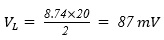 (3)
(3)
If ten bits of this IC are changing simultaneously VL = 870 mV.
The STM32F4 used in the LCD driver PCBA is using a 176 pin LQFP package with inductance in the range of 7 nH to 10 nH per pin [2]. As previously shown by Figure. 7, the ground bounce measured on the STM32F4 MCU was ~780 mV. The STM32F4 datasheet specifies di = 5 mA max per IO line. Thus the inductance per pin from the measured ground bounce value can be calculated. Ideally the intent is to find a correlation to the measurement if the calculated inductance is close to the datasheet specified inductance numbers. Assuming dt = 1 ns, using di = 5 mA and VL = 780 mV thus the total package inductance is calculated as
 (4)
(4)
Therefore, the inductance per pin can be approximated by dividing by 24 bits active during the 780 mV measurement captured.
 (5)
(5)
This correlates to the ~7 nH of 176 pin LQFP package with 24 bits switching for the RGB LCD interface.
Unfortunately, the LCD manufacturer was not ready to change the IC package. So we had to move forward to other possible solutions.
Solution 3: Differential signals for the display interface
The third option was to use a differential signaling interface to the display as an alternative to the parallel RGB interface. The logic state changes in the differential circuit are opposite of each other, so the current that flows from the power supply remains steady. This is one of the more significant advantages of differential signaling over single ended signaling. The magnitude of current flowing through the power leads of the IC package remains constant. As a result, the supply and ground bounce of SSN that develops across the inductance in the power leads is zero [1].
The robotic system was updated with a new LCD display, which used a differential signaling interface. A Renesas Synergy microcontroller, with a 176 pin LQFP package (with typical parasitic inductance of ~7nH to 10nH) is used in the LCD driver PCBA. The EMI response shown by Figure. 12 compares the new LCD display against the original LCD display Rev A, which has ground bounce. The LCD Rev A with supply and ground bounce showed multiple noise peaks crossing the CISPR class B limit (red line shown in Figure 12). The new LCD display, with differential signals, showed only a few noise peaks were crossing the CISPR class B limit (lower red line on Figure 12). This showed ~20 dB improvement compared to the original LCD display Rev A version. With the updated LCD display, the EMI emission peaks are well within the CISPR class A limit (upper red line on Figure 12, image on the right).

Figure 12: 3-meter EMI measurement – Front Horizontal – LCD Display Rev A (left) vs. new LCD display with differential signaling (right)
As shown, differential signaling is a very good solution to reduce EMI generated from supply and ground bounce. The only drawback being that differential signaling requires two wires, two connector pins, two drivers, and two receivers, which adds extra cost to the design.
Conclusions and Summary
The EMI issues created by these ICs at the device level can be coupled into the PCB and then into the system. These EMI issues will cause product delays as well as additional compliance testing costs to be incurred. The frequencies involved in the switching transients are too high for discrete capacitors to support, due to inherent inductance of the IC package. Adding plane capacitors to filter the high frequency noise only provides a partial solution to these types of problems. If the design extra cost is acceptable, differential signaling is a proper solution to mitigate supply and ground bounce. As a tradeoff, it is these switching transients that can also compel the designer to use BGA packages with lower parasitic inductance.
References
[1] Lee Ritchey, John Zasio,and Kella Knack, Right the first time: a practical handbook on high-speed PCB and system design, Speeding Edge, 2003, Vol. 1.
[2] D3uzseaevmutz1.cloudfront.net. [online] Available at: https://d3uzseaevmutz1.cloudfront.net/pubs/misc/PackageGuide5.pdf
[3] Eric Bogatin, Signal and power integrity simplified, Prentice Hall, 2010.
[4] About Ground Bounce and How to Measure It. Available at: https://blog.teledynelecroy.com/2018/08/about-ground-bounce-and-how-to-measure.html
[5] Lamson, Michael, “Packaging Takes Center Stage in IC Design Process” Electronic Design, June 8, 1998. Shear, David “Ground Bounce Tests Revisited” EDN, April 1993.