
Skew can come from any intra-pair asymmetries, such as: packages, ball grid array (BGA) breakouts, intra-pair routing length mismatches, connectors, and asymmetrical return path vias to name a few examples. Many of these can be controlled by specifying tight constraints in the design. But, since FWE is statistical in nature, it can be difficult to control the timing skew it causes and, at these data rates, it can ruin your day.
FWE skew is the term commonly used when a fiberglass reinforced dielectric substrate causes intra-pair timing skew of the same length. Since the dielectric material used in the printed circuit board (PCB) fabrication process is made up of glass yarns woven into cloth and impregnated with epoxy resin, it becomes non-homogenous.
As illustrated in Figure 1, when the top trace is routed over an area of low resin fill glass weave for a portion of its length, it has a different propagation delay compared to the bottom trace routed over an area of high resin fill glass weave. The difference in delay is known as timing or phase skew.
The speed at which a signal propagates along a transmission line depends on the material’s relative permittivity (er), also known as dielectric constant (Dk). The higher the Dk, the slower the signal propagation. Since modern serial link interfaces use differential signaling on a pair of transmission lines of equal length, any timing skew between positive (D+) and negative (D-) signals converts some of the differential signal into a common signal component. Ultimately, this results in eye closure at the receiver and contributes to electromagnetic interference.
 Timing skew in the time domain manifests itself as a resonant null in the frequency domain, as shown in Figure 1. In this example, if the timing skew is equal to one-half unit interval (UI) of the baud rate, D+ and D- signals are shifted 90 degrees and the resonant null occurs at the frequency of the baud rate.
If the intra-pair timing skew (tskew) and FWE lengths are known, the resonant frequency (f0) can be predicted using the following equation:
 (1)
(1)
where:
 seconds per unit length
lengthFWE = maximum FWE length
c = speed of light = 2.998E+8 m/s (1.18E+10 in./s)
Dkmin, Dkmax are the minimum and maximum effective Dk due to the glass weave.
When TDskew is equal to 1UI, D+ and D- signals are shifted 180 degrees and become in phase with one another. The resonant null occurs at the Nyquist frequency, equal to one-half of the baud rate, and the eye is totally closed.
 (2)
(2)
By definition, the baud rate is the number of symbols transmitted per UI. For non-return-to-zero (NRZ), the baud rate equals the symbol or bit rate. For pulse amplitude modulated 4-level (PAM-4) signaling, there are two symbols per UI and the baud rate is one-half the bit rate. So, for 56 GB/s PAM-4, the baud rate is 28 GBd. For the IEEE802.3bs, Ethernet 400 G standard, the baud rate is 26.56 GBd, PAM-4 and is used for this study.
The skew issue is exacerbated for PAM-4 signaling (see Figure 2). In these examples a simulated1 lossless transmission line is used to show the effect of eye closure due to skew. Of course, there is no such thing as a lossless transmission line, but it is a useful method to isolate loss strictly due to skew. As shown in Figure 2a, with 0 UI of skew, the channel loss is flat and eyes are wide open.
A resonant null in the frequency domain, due to FWE skew, behaves like a notch filter. Depending on the Q-factor, frequencies near resonance are attenuated. If the resonant null occurs near the Nyquist frequency, the eye is reduced. In the example of Figure 2b, with 0.5 UI, or 18.8 ps of skew, there is a resonant null at the baud rate and the insertion loss is 3 dB at the 13.28 GHz Nyquist frequency. This causes an eye height (EH) reduction of 153 mV and an increase of 10 ps of jitter.
When skew is 1 UI, or 37.65 ps, as shown in Figure 2c, the resonant null is at the Nyquist frequency and the eyes are totally closed. With a lossy channel and other impairments, eye closure will only get worse.

TOTAL SKEW BUDGET
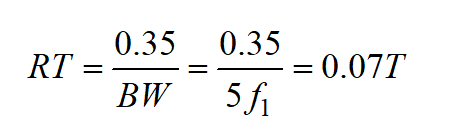
As a rule of thumb, we usually strive for an interconnect bandwidth (BW) five times the Nyquist frequency of the bit rate. This follows many oscilloscope manufacturers’ specifications for a risetime (RT)-BW product equal to 0.35, i.e.
 (3)
(3)
Five times Nyquist represents the fifth harmonic sinusoidal component of a Fourier series. An interconnect BW up to the fifth harmonic preserves the integrity of the risetime down to 7 percent of the period (T) of the fundamental frequency (f1).
 (4)
(4)
Some industry standards limit the total skew budget in a channel to 0.2 UI from all sources. But is that enough for today’s PAM-4 systems? Twenty percent of a UI results in a resonant null at a frequency (f0) equal to five times the Nyquist frequency (fNq).
If,
 (5)
(5)
Then,
 (6)
(6)
At 26.56 GBd that is only 7.53 ps.
But, 0.2 UI would obliterate the fifth harmonic of the Nyquist frequency. Historically, for NRZ and lower baud rates, there was more margin, but for PAM-4, with a -9.5 dB signal to noise (S/N) penalty, 0.2 UI may further strain channel margin.
For that reason, a good rule of thumb to follow is to ensure that the first null occurs at the seventh harmonic of the Nyquist frequency to maintain the integrity of the fifth harmonic frequency component. This means a total skew budget of 0.14 UI.
 (7)
(7)
Figure 3 compares 0.2 UI and 0.14 UI total skew budgets vs. common industry standard baud rates. As shown, there is an exponential decline in skew budget as baud rate increases. For 0.14 UI, the total skew budget at 26.56 GBd is 5.27 ps, and at 56 GBd it is only 2.5 ps. Since this is the total skew budget, it does not leave much left for the FWE skew budget.

Figure 4 compares two lossless differential pair simulations with 0.14 UI (see Figure 4a) and 0.2 0UI (see Figure 4b) of skew added. The eye diagrams show that with 0.22 dB delta in insertion loss at 13.28 GHz Nyquist, there is an additional 12 mV of reduction in center EH and an increase of 0.57 ps of jitter due to the resonant null shift in frequency down to 66.4 GHz (see Figure 4b).

THE REALITY
For a lossless channel, 12 mV seems insignificant. But that is not reality. Real channels have loss and other impairments that further erode the eye opening. Furthermore, many specifications have limits on total loss.
The IEEE 802.3bs chip-module (C2M) specification2 has a tight insertion loss (IL) mask requirement of 10.2 dB at 13.28 GHz. Table 120E-1 of the same document specifies a minimum differential EH of 32 mV and an eye symmetry mask width (EW) of 0.22 UI or 8.23 ps at TP1a.
Figure 5 shows simulated results of IL and PAM-4 eye diagrams for a realistic chip C2M channel. Worst case, power-voltage-temperature (PVT) is used for the transmitter model including the package. Figure 5a shows results for the inherent channel, with all impairments included. It has 1.7 ps, or 0.045 UI of skew, as a baseline. The channel loss just meets the IL mask and the eyes meet the IEEE 802.3bs EH and EW with margin.
Figures 5b and 5c show total skew to the equivalent of 0.14 UI and 0.2 UI, respectively. As skew increases, IL degrades due to a decreasing resonant null frequency. At 0.14 UI (see Figure 5b), IL is just starting to violate the IL mask near the Nyquist frequency break point and the EH and EW are still within specification. At 0.2UI (see Figure 5c), IL is slightly worse and the EH just fails the 32 mV specification, but it passes the EW specification.
The minimum eye heights and widths measured at 10-5 bit-error-ratio (BER) are:
a) 0.045 UI: (37; 37; 37) mV and (9.601; 9.789; 9.601) ps – EH/EW – PASS
b) 0.14 UI: (35; 34; 34) mV and (9.224; 9.601; 9.224) ps – EH/EW – PASS
c) 0.20 UI: (31; 30; 30) mV and (9.036; 9.036; 9.036) ps – EH – FAIL/EW – PASS

FWE SKEW BUDGET
Since FWE is a function of glass weave style, resin chemistries, trace geometries, and stackup parameters to name a few things, it is difficult to establish an exact delta Dk from data sheets. A practical study3 showed a maximum FWE skew of 45 ps, over 7.5 in. This represents 6 ps/in. of FWE skew. The boards were designed in stripline using double layer 1035 spread-weave glass for the Megtron-6 cores and prepregs.
This is a realistic study for modern multi-gigabit designs, but, the complexity of multi-ply layups does not ensure perfect alignment of the glass bundles of each ply above and below the traces. In fact, observations of cross sections show glass bundles of each ply offset from each other, which would improve FWE skew results. Following the methodology of Simonovich4 gives a more pessimistic 9.46 ps/in., which might be seen in microstrip with single layer construction.
If 1 ps of skew is budgeted for all impairments, such as length matching, connectors, and breakouts, a FWE skew budget for various baud rates can be established. Figure 6 plots FWE UI skew budget vs. baud rate assuming a total skew budget of 0.14 UI. Up to 10 GBd or so, the 1 ps of skew from other impairments is negligible. After 10 GBd, however, it starts to impact the FWE skew budget. At 26.56 GBd and 32 GBd it is approximately 0.11 UI, and at 56 GBd it is only about 0.08 UI.

With 6 ps/in. of FWE skew,3 the FWE lengths are calculated to meet a 0.14 UI total skew budget and are plotted vs. GBd rate (shown as the red bars in Figure 7). If 9.46 ps/in. is used, following the methodology from Simonovich,4 the FWE lengths are shown in blue.

It is evident that there is an exponential decline in FWE length for an exponential rise in GBd rate. Above 10 GBd, FWE becomes increasingly more difficult to control without further mitigation techniques. At 26.56 GBd and 6 ps/in. of skew, the maximum length is 0.7 in.; at 56 GBd, it is only 0.25 in. But for 9.46 ps/in. of skew, the lengths reduce to about 0.5 in. at 26.56 GBd and 0.2 in. at 56 GBd.
Popular FWE skew mitigation techniques include:
- A glass style where the glass strands are mechanically spread to fill in the resin rich windows
- Zig-zag or random routing of differential pairs
- A differential pair pitch to line up with glass style pitch. However, this is not always practical because the warp and fill yarns in different glass styles may have different pitches
- Artwork rotated 7 to 10 degrees on the PCB panel
SUMMARY AND CONCLUSIONS
With bit rates above 25 GB/s, a 0.2 UI total skew budget has shown to be insufficient for PAM-4 signaling for some industry standards. To mitigate the effect of skew on EH and EW, it is proposed that 0.14 UI be used for a total skew budget to maintain a channel bandwidth of at least seven times the Nyquist frequency of the baud rate.
Up to 10 GBd or so, limiting the non-FWE skew to 1 ps from other impairments has a negligible effect on a 0.14 UI total skew budget. But, after 10 GBd, it starts to reduce the FWE skew budget. At 26.56 GBd and 32 GBd it is approximately 0.1 UI and at 56 GBd it is only about 0.08 UI.
Larger and larger switch application specific integrated circuit (ASIC) packages with tighter and tighter BGA pitch packages means reduced impedance-controlled line widths and space to break out of the BGA pin field. The challenges are similar for routing through tight pitch backplane connectors. It is not uncommon to see BGA escape lengths on the order of 0.25 in. or more; and, in most cases, those breakouts are parallel to X-Y axis of the panel. At 56 GBd, this represents the entire skew budget and becomes unmanageable without further FWE skew mitigation techniques.
Of course, this analysis is based on worst case, and does not necessarily mean that a violation of this skew budget will cause the system to break, but it does show that more detailed modeling and simulation of the channel is required with perhaps more consideration to include a FWE skew budget in the channel model. This will present severe challenges for the design of next-generation 112 GB/s systems and the selection of PCB dielectric material.
REFERENCES
- Keysight Pathwave Advanced Design System (ADS) Circuit Design and Simulation Software, Version 2021, Update 2, Web, www.keysight.com/en/pc-1297113/advanced-design-system-ads?cc=US&lc=eng.
- IEEE Std 802.3bs™, The Institute of Electrical and Electronics Engineers, New York, NY, 2017.
- B. Gore and S. McMorrow, “Vehicle for Insitu Glass Fabric Characterization,” EDICON, September 2017.
- L. Simonovich, “Practical Fiber Weave Effect Modeling,” White Paper, Issue 3, Lamsim Enterprises Inc., March 2011.
Published in the SIJ 2022 Print Issue, Technical Feature: Page 24.