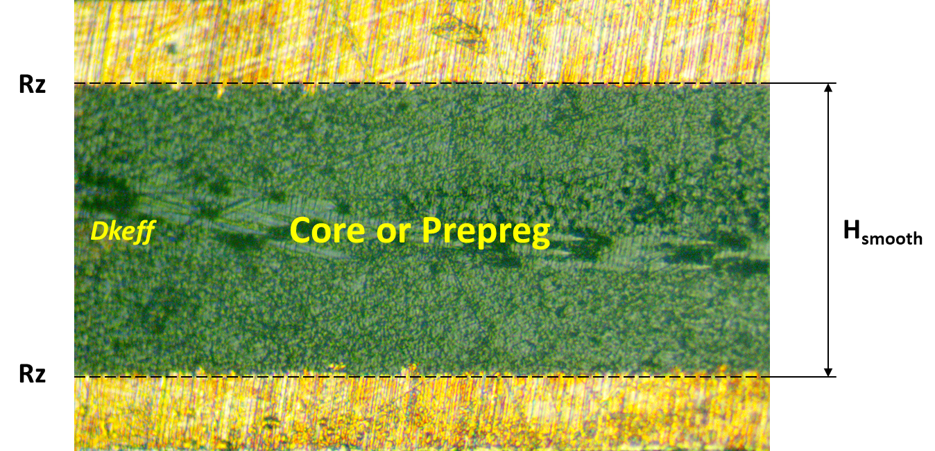
In part one of my Signal Integrity Journal article, “A Tale of Two Data Sheets and What You Need to Know About Dielectric Constant (DK)” [1], I explained how air entrapment, due to IPC-TM-650-2.5.5.5 test method manual [7], is the primary reason for effective dielectric constant (Dkeff) and phase delay discrepancies between simulation and device under test (DUT) measurements. Entrapped air of the test fixture results in a lower Dk published in laminate suppliers’ Dk/Df tables than what would be measured in a real printed circuit board (PCB) application. This is because in a real PCB, everything is bonded together with no air entrapment, as shown in a cross-section view of Figure 1.

Figure 1. Example of foil bonded to core or prepreg dielectric. Rz is 10-point mean roughness of foil as measured by a profilometer. Hsmooth is the thickness of the dielectric as if the foil was removed.
When copper foil with the same Rz roughness is bonded to each side of the core or prepeg, Dkeff is determined heuristically from published Dk by this simple correction factor [1]:
Equation 1.

where:
Hsmooth is the thickness of the dielectric as if the foil was removed
Dk = Dielectric constant published in laminate suppliers’ Dk/Df tables
Rz = 10-point mean equivalent to Rz(JIS) or Rz(DIN) published in foil suppliers’ data sheets. This is not to be confused with Rq, which is RMS value of roughness.
Rogers Corporation [4] understands this. That’s why they provide the “design” Dk in addition to their bulk Dk, as measured by TM650 clamped stripline resonator test method [7]. Design Dk is an average number using a differential phase length method from several different tested lots of material and on the most common thickness. This method is based on measuring phase difference from two identical microstrip transmission line geometries, of different lengths on the same panel. Because this is a real microstrip application, the dielectric is fully bonded to the copper and there is no air entrapment. Knowing the phase and length difference, the effective Dk is empirically determined.
The accuracy of the resultant effective Dk depends on several factors like:
- fixture design
- length ratio between two transmission lines
- material thickness of the sample under test
- the thickness of the copper
- actual roughness of the foil on the microstrip circuit.
In lieu of actual Dk/Df tables, Rogers provides a handy impedance calculator as shown in in the RO4003C example of Figure 2. There are three Dk options available to use:
- Z-axis bulk Dk
- Dk values for specific frequencies
- Dk values for characteristic impedance
The first radio button, as shown in Figure 2, gives the z-axis bulk Dk value of 3.55, as measured by TM650 2.5.5.5 test method manual. However, the value does not change when different frequencies are selected. This makes the number suspect since clearly design Dk does change over frequency. Thus this number can be considered equivalent to marketing data sheets, and should not be used.
When the middle radio button is selected, a Dk value for a specific frequency is displayed, which corresponds to a frequency entered in the lower right frequency box of Figure 2. This is the most useful option, since it allows the user to choose the right design Dk at whatever frequency they choose for their application, including characteristic impedance. This option already factors in the foil roughness effect, so no correction factor is needed to use in your simulator.
The last radio button selects a Dk for characteristic impedance calculation. It is a “design” Dk with yet a different Dk. Similar to the Bulk Dk option, it does not change over frequency. For any simulation tool other than the Rogers’s calculator, Bulk Dk and Dk values for characteristic impedance values should not be used.

Figure 2. Example of Rogers Corporation impedance calculator. For an 8-mil thick RO4003C dielectric, bulk Dk is 3.55 while design Dk over frequency is shown in bottom left window.
Under the information tab, the user can download design Dk over frequency, for a specified thickness, shown in the bottom left window of Figure 2. This data can be selected and copied to the clipboard and pasted into a spreadsheet for further processing.
Figure 3 plots design Dk vs. frequency for various thickness from 8 mils to 60 mils for RO4003C material. As can be seen, design Dk is not constant over frequency and furthermore it is different for different thicknesses, mainly due to the roughness of the foil that is already included in the measurement.
Thinner materials have a higher design Dk than thicker materials for the same roughness of foil. This is because when the foil teeth protrude into a thin dielectric material, there is a higher concentration of e-fields, resulting in higher capacitance between top and bottom copper layers. For thick dielectrics the foil teeth have less of an impact on capacitance and thus Dkeff, as described mathematically by Equation 1.
Since the roughness of the foil does not significantly influence the design Dk for thick laminates, we can assume the bulk Dk is roughly equivalent to design Dk over frequency for the 60-mil laminate.

Figure 3. Design Dk vs. frequency for various thickness of RO4003C from 8 mils to 60 mils mainly due to the roughness of the foil. Thinner material has a higher design Dk than thicker material, for the same roughness of foil.
Heuristically, we can rearrange Equation 1 and estimate the Rz roughness of the foil used on RO4003C laminate to be 6.302 μm from Equation 2.
Equation 2.
 where:
Hsmooth is the thickness of the 8 mil (203 μm) laminate
DkBulk = 3.55 at 60 GHz for 60 mil (1524 μm) laminate
Dkeff = design Dk of 8 mil (203 μm) laminate at 60 GHz
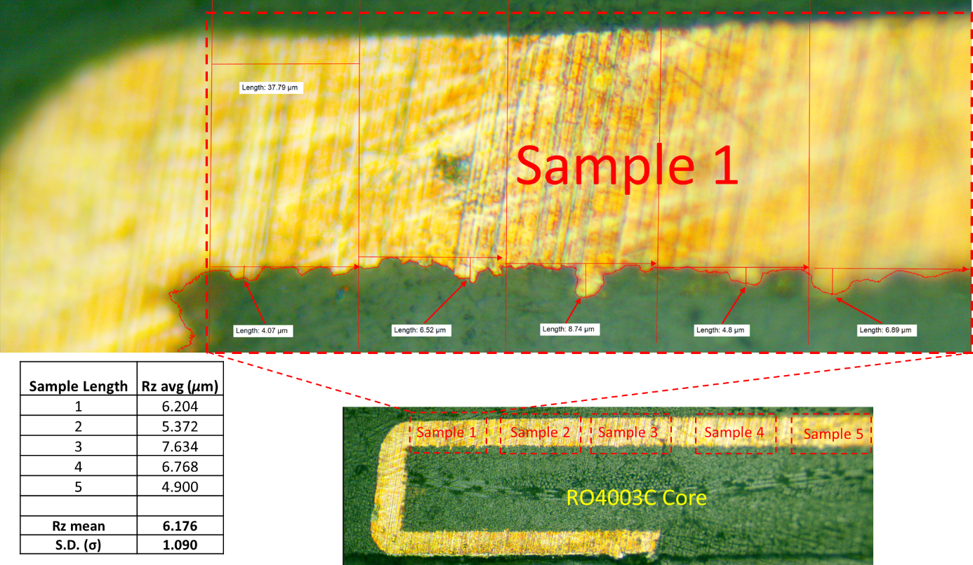
A cross-section sample from a time domain reflectometry (TDR) demo board, courtesy of Picotest [6], was measured and is shown in Figure 4. The TDR demo board was fabricated with 8-mil thick Rogers RO4003C core laminate and cladded with 2 Oz copper foil.
Five highlighted random sample lengths of copper roughness, labeled Sample 1 to Sample 5 of Figure 4, were analyzed. The total length of each respective sample was then partitioned into five equal sections, similar to the blow-up picture of Sample 1, to measure the maximum peak to valley height of each section. The five measurements of each sample length were then averaged to determine the Rz roughness, as described under IPC TM650 2.2.17A [8] and shown in the table of Figure 4.
The mean value of Rz for the five samples was 6.176 μm with a standard deviation (SD) of 1.090 μm. This compares favorably with the estimated roughness of 6.302 μm, determined from Equation 2.

Figure 4. A cross-section sample from a Rogers RO4003C based TDR demo board, courtesy of Picotest [6], used to determine Rz roughness of the foil.
When we use the actual roughness measured from Figure 4 and Equation 1, we can then calculate Dkeff at 60 GHz for different thicknesses, shown in Table 1. As can be seen there is, less than 1% delta compared with design Dk reported from the calculator!
Table 1. Comparison of Roger’s Design Dk vs. Dkeff when simple correction factor applied to Bulk Dk at 60 GHz.
Height |
Height |
Bulk Dk |
Design Dk |
Rz |
Dkeff |
Delta |
8.0 |
203 |
3.550 |
3.785 |
6.176 |
3.780 |
-0.13% |
12.0 |
304 |
3.550 |
3.702 |
6.176 |
3.700 |
-0.04% |
16.0 |
406 |
3.550 |
3.657 |
6.176 |
3.661 |
0.12% |
20.0 |
508 |
3.550 |
3.625 |
6.176 |
3.638 |
0.37% |
32.0 |
812 |
3.550 |
3.580 |
6.176 |
3.605 |
0.69% |
60.0 |
1524 |
3.550 |
3.550 |
6.176 |
3.579 |
0.82% |
- B. Simonovich, “A Tale of Two Data Sheets and What You Need to Know About Dielectric Constant (DK),” Signal Integrity Journal article, April 2022.
- L. Simonovich, "A Practical Method to Model Effective Permittivity and Phase Delay Due to Conductor Surface Roughness," DesignCon 2017, Santa Clara, USA.
- Isola Group, 6565 West Frye, Chandler, AZ 85226.
- Rogers Corporation, 2225 W. Chandler Blvd., Chandler, AZ 85224.
- J. Coonrod, “Managing PCB Materials: Dielectric Constant (Dk)”, Rogers Corporation, Blog Article, Sep 11, 2018.
- Picotest, Phoenix, AZ 85085.
- IPC-TM-650, 2.5.5.5, Rev C, Test Methods Manual.
- IPC-TM-650, 2.2.17A, Test Methods Manual, “Surface Roughness and Profile of Metallic Foils (Contacting Stylus Technique).”
- Bereskin, A. B. “Microwave Dielectric Property Measurements”, Microwave Journal, vol. 35, no.7, pp. 98 – 112.

