
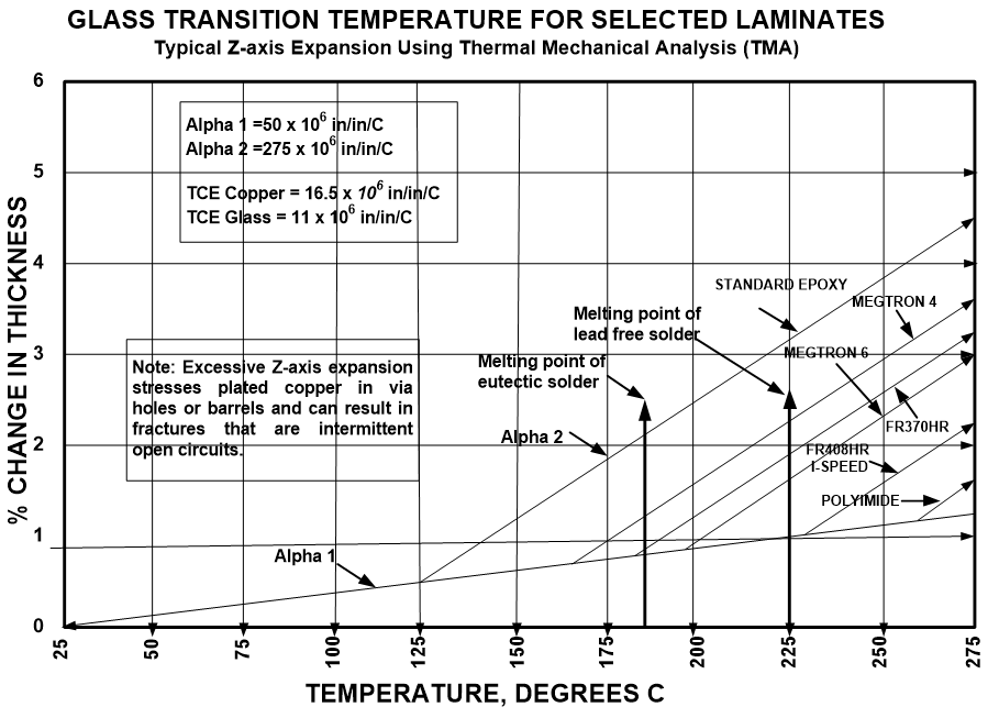
Glass transition temperature, Tg, is a property of resin systems that is the temperature at which a resin system changes the rate of expansion with temperature from a low level to a very high level. Figure 1 is a graph showing how several common laminate systems behave with rising temperature.
The term “glass” in the context of this discussion does not refer to the glass weaves in a printed circuit board but, rather, it is a material science term for any material that does not exhibit a crystalline structure. Glass is one such material, as are many other substances.
Notice in Figure 1 that there are two different coefficients of thermal expansion, Alpha 1 and Alpha 2. Where the slope changes is defined as the “glass transition temperature”, Tg. Most resin systems have an Alpha 1 about what is plotted in Figure 1. This rate of expansion is low enough that the operating temperatures of most electronic products see no ill effects from this volume growth as temperatures change during operation.
When the temperature rises above the Tg, the rate of volume expansion increases dramatically, as can be seen in Figure 1. Printed circuit boards are reinforced in both the X and Y axes by the glass and copper layers of the PCB. The temperature coefficients of expansion of these are listed in Figure 1 and are similar to resins below Tg. Because of this, all of the volume expansion of the resin system must go in the Z axis. The plated through holes and vias are oriented in the Z axis.
Plotted on the graph is the melting point of eutectic solder, 185°C. The Alpha 2 for the original epoxy-based laminate systems is also plotted. As can be seen, the volume expansion is quite large at the time of wave soldering. When the industry began to design PCB stackups that were 90 mils (2.2 cm) and thicker, it was discovered that vias were stretched during wave soldering to the point that they failed or fractured. Figure 2 is an illustration of this.
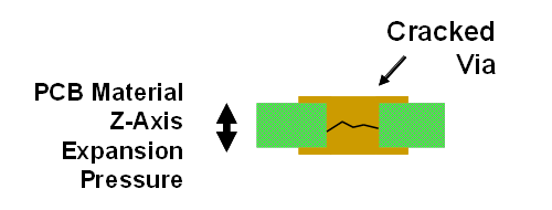 Figure 2. Cracked via cross-section.
 Once the PCB cools down to room temperature, the resin shrinks back to its original thickness and the via becomes continuous again, resulting in a fully functional PCB. As the PCB heats up during operation, the resin expands and the via becomes an open circuit again, thus creating a failure. The failed PCB is returned to the factory where it tests well again. Back to the field it goes, and back to the factory it returns after failing again. These were known as “boomerang” or “rubber band” PCBs.
Solving the failed via problem gave rise to the “High-Tg” movement. Manufacturers of the resin systems adjusted their formulas to move the Tg to at or above the melting point of solder. Megtron 4 and FR370HR are examples of this. Materials of this type worked very well until the “lead-free” standard was adopted. As can be seen from Figure 1, the melting point of most lead-free solder is about 225°C. Using Megtron 4 and FR370HR resulted in the failure of cracked vias in thick boards all over again.
Once again, the manufacturers of resin systems went to work developing resin systems with ever higher Tg. FR409HR and other resin systems like it were developed to solve the via cracking problem again. Manufacturing thick PCBs has not suffered from cracked vias as a result of resin expansion for quite some time.
As with most things, new problems develop that were not foreseen. Figure 3 is a cross section of a triple-high stacked blind via.
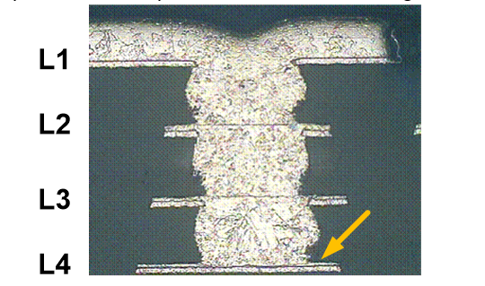 Figure 3. Cross-section of a three high stacked blind via.
These types of vias are used extensively in avionics and satellites. Avionics in fighter jets can experience temperature changes from below freezing to well over 150°C in very short time periods. These events occur hundreds of times in the life of the product containing these vias.
The bond between the blind via from L3 and L4 to the copper foil on L4 (depicted by the yellow arrow) is put under stress as the resin system in the three laminate layers above it expand with the rising temperature. Even though the temperatures are below Tg, the Z axis expansion pulls on this bond with enough force that some of these bonds are broken at the high temperatures, resulting in an open circuit. The failed PCB is returned to be repaired, as with the failures described previously. It cools down, the open circuit closes back up, and PCB is functional.
Currently, the only solution is to use the thinnest laminates possible for the build-up layers and drill extra-large blind vias to increase the area of the bond, or to use offset blind vias, as shown in Figure 4.
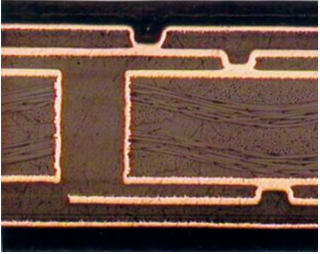 Figure 4. Offset blind vias.
The downside of using offset blind vias is a more complex design process. There is also the possibility that there will not be enough room use this approach in very dense designs.
Summary
The expansion of the resin systems in laminates has been a source of reliability problems as the electronics industry has placed ever higher demands on those used in printed circuit boards. Suppliers of these resin systems have improved their resin systems to eliminate or minimize failures from expansion as the systems using the PCBs have been made more complex and subjected to ever harsher environments. Currently, the only technologies that still suffer failures from resin expansion with temperature are triple-high stacked blind vias.