
Internet of Things (IoT) has become the new buzz words to refer to connecting all devices to the internet. According to Forbes, the IHS Markit Group estimates there was an installed base of 15 billion IoT devices in 2015 with an expectation of a 15% compound annual growth rate (CAGR). Other estimates are as high as a 35% CAGR. By 2020, there could be as many as 50 Billion IoT devices.
While IoT encompasses everything from cars and buildings to watches and pacemakers, this design guide focuses on the low end of IoT devices, with small form factor and low energy consumption. Even though these sorts of products are not in the same performance class as server motherboards, not paying attention to signal and power integrity design principles at the beginning of the design cycle may require multiple board spins to get your IoT product working.
In this design guide, we focus on the best design practices for:
- a two-layer board
- with an RF component
- with a micro controller and other digital devices
- with an analog to digital converter (ADC)
- designed for low cost
- designed for low energy consumption
If we don’t do anything special in the design, but assume the interconnects are transparent, and just design for connectivity, the product may still work. After all, many products are shipped based on this approach.
Without numerical analysis of the magnitude of the problems expected, we can never be 100% sure the product will work the first time. But by following these best design practices, we are reducing the risk and increasing our luck that the design will work. When the best design practices are free and do not add manufacturing or BOM costs, they should become habits as part of a “risk reduction” process.
Tradeoff analysis using rules of thumb, approximations and numerical simulations are the most efficient way of performing the cost-performance-risk tradeoffs before the product is built and giving a higher chance of first article success.
As a design strategy, we can always “buy insurance” by paying more to over-design the product to add performance margin. This reduces the risk even further and gives us a better chance of it working the first time. Cost reductions can come after the product is released.
The general process we use in establishing the best design practices to reduce risk is to identify the potential problems that could arise and engineer design practices to reduce their magnitude.
Here are ten recommended best design practices and a few examples of doing it right, and doing it wrong.
Design for good signal integrity
Use devices with as long an edge transition time as possible, consistent with the timing performance required. Often times you don’t have any control over this feature, but look for it. At the least, know the rise time of all of your signals.
The bottom layer of the board should be a continuous ground plane. If you split the ground plane, you should have a really strong compelling reason, other than someone told you to. Splitting the ground plane 99.9% of the time causes more problems than it fixes.
If you do need to add a cross under in the ground plane make it as short as possible and do not route signals over the split.
Even if you don’t need it, always route signal lines as controlled impedance transmission lines. This means use a continuous ground plane underneath the signal lines. NEVER cross a gap in the return path (see the section on preventing ground bounce.)
Use as narrow a line as your fab vendor can do at no cost premium. This means the characteristic impedance will be higher than 50 Ohms. This will reduce the power consumption in charging and discharging interconnects. If the interconnect density is low, route the signal lines as far apart as practical to minimize cross talk. Only route lines close together when you need to. (see the section on cross talk.)
If the interconnect traces are shorter, in inches, than the rise time in nsec, you may not have to terminate the lines. For example, if the rise time is 3 nsec, traces 3 inches or shorter may not require termination. When in doubt, do a simple simulation modeling the interconnects as uniform transmission lines. But, you need to know the output impedance of your drivers. If you don’t know it, assume worst case they are 10 Ohm output impedance. Pay particular attention to clocks’ edges as most devices are strobed by edges. Always a good policy to simulate at least the clock nets.
If the traces are long enough that they require termination, use source series termination when possible. This will be the lowest power consumption. Don’t even consider far end termination if you live for lowest power consumption.
The best routing topology of signals is point to point. Always use point to point when possible. The alternative is use a daisy chain with as short a stub to the individual receivers as possible. Even if you have to make your signal line meander around, use a daisy chain to avoid any branch topology. When in doubt do a simple SPICE simulation to see the magnitude of the reflections. If you don’t need the short rise or fall time, use a small series RC filter at the source to increase the rise or fall time to reduce the impact from the reflections, and reduce the current into the signal line.
Design for low cross talk
Even though all the signal lines are designed as controlled impedance lines, there will be line to line cross talk. It will manifest as near end cross talk and far end cross talk. If the lines are 50 Ohms, and the spacing is the same as the line width, there will be about 5% near end cross talk between adjacent lines. If the line impedance is as high as 100 Ohms, and the spacing is equal to the line width, the near end cross talk can increase to as much as 20%. The spacing should be 5x the line width for 5% near end cross talk for high impedance lines.
Far end cross talk will only arise in surface, mirostrip traces. The far end crosstalk will scale with the coupling length and inversely with the rise time. With 50 Ohm lines and a spacing the same as the line width, the far end cross talk from adjacent traces will be 0.7% x Length[in]/RT[nsec]. If the signal rise time is 1 nsec and the coupled length is 2 inches, the FEXT will be 1.4%. Probably not something to worry about, but put in the numbers anyway.
If you use higher impedance than 50 Ohms, use a field solver to calculate the line to line FEXT and the closest acceptable spacing to use in a bus.
Design for test
Some signal lines should be selected for probing with an oscilloscope or for in circuit testing. Here are four considerations when designing for test:
- Don’t load the signal line. Keep the test point connection with as short a stub from the signal line as possible.
- Use as small a capture pad for the probe location as possible. Use silk screening to identify probe points.
- When the signal is propagating on the line, not every point on the signal line is equivalent. Select the location of the probe point as close to the RX end as practical.
- When probing a signal line, you also want to select an adjacent point as a return connection for the probe. Look at the footprint of your probe tip and use a pitch between the signal and return connection to match the probe. If the return path is the plane below, drop a via to the plane in the return pad.
Design for probing with a scope
The goal of probing with a scope is to not load the signal line and to maintain the bandwidth of the signal up to the scope. The probing system and scope bandwidth should be at least twice the signal bandwidth. If the signal has a 3 nsec rise time, its bandwidth is about 100 MHz. The scope and probe’s bandwidth should be at least 200 MHz. This means the sample rate of the digital scope should be at least 1 GSps.
The scope probe should not load the line. This means use a high impedance scope probe. Many are available at 1x or 10x with 1 Meg Ohm input impedance or higher and have a bandwidth > 300 MHz. However, they typically have an input capacitance of as much as 15 pF. Given your driver’s strength, you need to evaluate whether the 15 pF of capacitive load will affect the signal on the line. If the output impedance of the driver pin is 35 Ohms, the rise time degradation from the scope probe will be about 35 x 15 psec = 0.5 nsec, probably not an issue.
Alternatively, a high bandwidth scope probe can be made with a 450 Ohm resistor in series with a 50 Ohm coax cable. The scope input should be 50 Ohm terminated. The load to the circuit will be 500 Ohms. If your driver can handle this load, this probe might be a high bandwidth alternative. If your drive output impedance is 35 Ohms, the voltage on the line with the probe attached is 500/535 = 93% of the actual value there.
The probe tip should be made with as low an inductance tip as practical. Don’t use a long, meandering ground clip lead. Many scope probes come with a short ground connection tip. This will reduce the inductance of the tip and not degrade the bandwidth, and more importantly, reduce any inductive coupling from stray magnetic fields around the board.
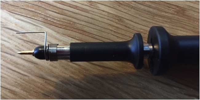
Figure 1, An example of a probe tip attachment using a closely space ground connection.
Design for reduced ground bounce
Ground bounce arises when the return path of signals are not uniform planes and return currents overlap in the same, narrow conductor paths. It commonly occurs in packages and connectors. There is little you can do about ground bounce in packages.
To not increase the ground bounce in packages, make any unused digital I/O pins in the package an output LOW and connect these I/O to the Vss connections. Just watch out for any chance the microprocessor might change the output to a HIGH during boot up or self-test.
Drop a via connection from the top surface of the package’s Vss leads to the ground plane with as short a lead as possible.
Alternatively, if the region under the package is not used, as with a peripheral leaded package, use a large pad under the package footprint with multiple vias to the ground plane below the package and route the ground package pins inward to the ground pad. Use as short and wide traces in the ground path as possible.
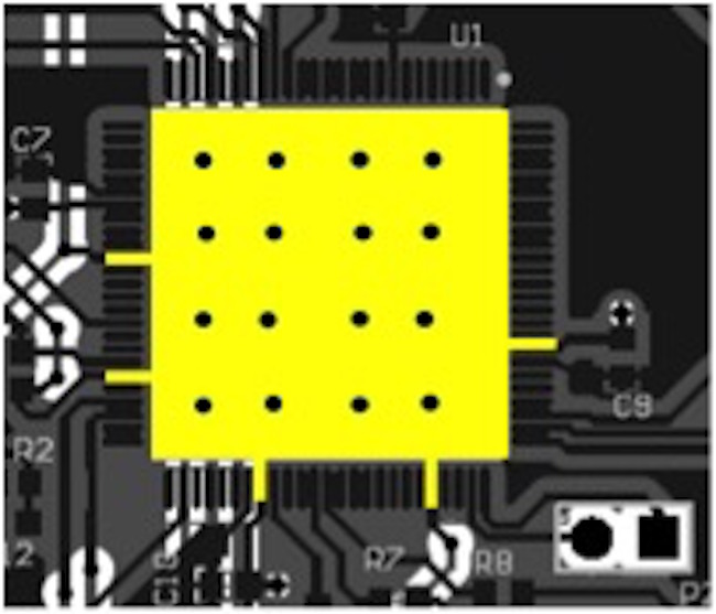
Figure 2. Example of the ground plane under the package, with vias to the plane below and package Vss leads connected.
When using connectors to ribbon or flex cables, interleave ground leads in the cables adjacent to signal lines. The lowest risk is to alternate G-S-G-S-G in the cables and the connectors for single-ended signals and G-S-S-G for differential signals. Fewer grounds may work but it is difficult to know for sure.
The second largest source of ground bounce is when signals cross splits in the ground plane on the bottom layer. Route signal traces around any splits in the ground plane beneath.
If a signal must cross a split in a ground plane, add a via on either side of the split, bringing a connection from the ground plane up to the top layer adjacent to the signal lines. Connect the vias on either side of the split with a 0 Ohm resistor adjacent to the signal lines. Use as short a connection in this 0 Ohm resistor path as practical. If a bus of signal lines crosses a split, separate the signal lines enough apart to route a 0 Ohm resistor between every signal line, if they will fit.
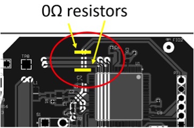
Figure 3. Example of two signal lines crossing a split in a plane below with adjacent 0 Ohm resistors providing a continuous return connection.
Design for low noise power distribution
For lowest power consumption, the Vcc will generally be as low as can be tolerated and generally there will be one Power Management IC (PMIC) and one power rail.
Generally, the core and I/O lines of the devices share the same power rails and Vcc pins. If there are separate core and I/O pins in the package, keep them separate until after the decoupling capacitor mounted to the Vcc pin. Then they can be bussed on the same power trace.
The goal for any power pin is to use as low an inductance capacitor mounted as close to the power pin as practical. Each capacitor will be connected between the Vcc pin and the Vss, or ground connection. Both connections- creating a loop- should be as short as possible. Drop a via to the Vss plane on the bottom of the board as close to the Vss pad of the capacitor as possible.
What size capacitor to use? Without knowing any of the details of the current requirements, pick the smallest body size capacitor you can assemble on the board, and the largest capacitance in that body size. Use at least one capacitor per Vcc pin. If more will fit, use more capacitors per power pin.
Usually, a PMIC and some sort of switch mode power supply will be used to regenerate the correct power rail voltage. This means there may be some periodic ripple on the power rail related to the pulses that drive the half bridge. These generally are filtered out by the LC circuit that is part of the SMPS. However, there are sometimes large currents in the inductor. These can couple as near field magnetic field lines to other structures on the board. For this reason, it’s best to use toroids to confine the magnetic fields, and to keep the SMPS components far from the sensitive signal lines.
Sometimes other voltages are created or sensed using resistor voltage dividers, sometimes with high impedance resistors. High impedance circuits are always more sensitive to AC capacitive pick up. Place the high value resistors as close to the sense pins as practical, with continuous ground underneath.
When sense lines are used as feedback for the output of a SMPS, route the sense lines as tightly coupled differential microstrip, far from any other digital lines. They should measure the Vcc as close to the usage point as practical.
If you have a device that is very sensitive to rail voltage noise and does not draw much current, or a specific power pin on a device for a PLL supply or ADC supply, you can add a ferrite bead in series with the power pin connection. Be sure to add the low inductance capacitor on the device side of the ferrite. This is the ONLY situation in which it might be acceptable to use a ferrite in the power path.
Route as wide a trace as practical between the Vcc pins and the Power Management IC (PMIC). This means design power traces for as low a characteristic impedance as practical, over a continuous ground plane on the bottom layer. It is okay to use a branched routing topology for the wide power traces. Shorter and wider power traces are better.
Estimate the series DC resistance in the power paths. A 1 ounce copper layer has a sheet resistance of about 0.5 mOhms/square. Count the number of squares in the power trace to estimate its series resistance. If the power trace is 25 mils wide and 1-inch-long, there will be 1/0.025 = 40 squares. The total resistance will be 0.5 mOhms/sq x 40 squares = 20 mOhms. If the current in this trace is 100 mA, the voltage drop will be 20 mOhms x 0.1 A = 2 mV. Is this acceptable voltage drop on the power rail in your application? Usually a rail can tolerate 50-100 mV drops.
Avoid the use of copper fill on the top layer, even if it is connected to ground. Instead, keep signal lines spaced apart and make power traces as wide as will fit. The wider the power traces, the lower their series resistance and the lower the inductance in their path.
Design for low energy consumption
Most of the energy consumed in an embedded application is in the microcontroller core. The very first step is to use as low a core voltage as you can get away with, but with enough margin to keep the voltage above the minimum when the core supply fluctuates.
When writing the code, it is useful to monitor the actual power consumption of the device to see what operations consume the lowest energy. For example, typically integer math will burn fewer joules than floating point math.
The ultimate energy source will be either a battery or some energy harvesting device using a super capacitor for local storage. These will feed a power management IC (PMIC) to provide the regulated voltage. The PMIC should be selected based on the average power burned and use as large a low inductance capacitor on the regulated voltage side to provide for the high current bursts.
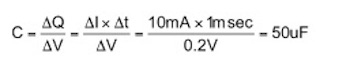
The size of the capacitor needed can be estimated based on the voltage drop allowed, ΔV, and the duration, Dt, of the current surge and the magnitude of the current surge, ΔI. For example, if there will be 10 mA current surges lasting for 1 msec and the voltage supply margin is 0.2 V from the regulated voltage level to the minimum voltage the core needs, the size of the capacitor on the core supply should be at least:
The capacitors distributed on each Vcc pin will also contribute to maintaining the voltage level and add design margin.
At the board level, the best that can be done to reduce energy consumption is to use interconnect traces with low capacitance. A 50 Ohm line in FR4 has about 3 pF/inch. If it is 2 inches long, it will be about 6 pF capacitive load. If a control or data line will have a 1.5 V signal on it and it will change at 1 MHz, the power dissipated because of one line is:
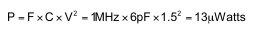
If there are 60 lines on the board, this is about 1 mWatt of power consumed in charging and discharging the board level interconnects.
For lowest energy consumption, use as short interconnects as practical and as high impedance as practical. Whenever you see high characteristic impedance lines, know they may have higher cross talk, so pay attention to this term as well.
Design for stable turn on
When the PMIC turns on, all the distributed capacitors have to be charged up. Generally, with a low output current PMIC, the inrush current can drive the power rail low, resulting in some devices turning off, some devices turning on.
The inrush current can be controlled by isolating the power traces to the higher current draw devices and using a series MOSFET as a power gate. Shunt it with a 10 k resistor which will act as a slow pre-charger for the decoupling capacitors. If there is 100 uF of capacitance, for example, the 10 k resistor will charge them in about 2 sec. After a controlled delay to pre-charge close to the Vcc level, the MOSFET can gate the rest of the VCC power to each device sequentially for stable and predictable turn on.
Design for low noise in the ADC
The analog to digital converter (ADC) is usually the most noise sensitive device on the board. It often connects to sensors either on the board or connected by external wires. Place the ADC as close to the sensor or edge of the board as possible to minimize the trace length on the board. Use as large a spacing between the analog lines as practical to reduce cross talk.
To further reduce cross talk, make the analog lines as wide as practical, consistent with the source impedance of the sensor and the time response required. Route the analog lines physically away from the digital lines, with a continuous return path underneath.
Usually, the package has a separate analog ground and digital ground pin. This is to prevent ground bounce noise from the digital signals coupling to the analog signals in the package. It is ok to connect both grounds to the same ground plane on the board.
If there is a separate Vcc pin for the analog side, this is a case where it is acceptable to use a ferrite bead in series with the Vcc power pin. Be sure to place the decoupling capacitor on the device side of the ferrite bead.
Design for low coupling to RF receivers
Place all the RF components on one end of the board, far away from digital lines and analog lines. It is ok to use the same continuous ground plane under the RF section as elsewhere in the board.
Consider placing the RF section on a separate board using a cable connection and only power, ground and digital control lines between them. Where possible, interleave the power and ground wires with the digital signal lines to reduce ground bounce.

Figure 4. Example of a separate RF module away from the digital control circuits.
If they are powered by the same supply as the other components, consider using a ferrite in the power path, as close to the RF region as possible, with a local decoupling capacitor as close as possible to the Vcc power pin of the RF device. This is to prevent noise from the power rail from getting onto the sensitive receiver amplifier of the RF device.
While following these best design practices will not be a 100% guarantee the product will work, these steps will reduce the risk of noise corrupting the intended application and increasing your chance of success.