3D integration came as a response to the requirements of high performance and small footprint electronic devices. Today, the need for more heterogeneous integration schemes with increased functionalities becomes more obvious as the three worlds of digital, analog/mixed-signal (AMS) and RF electronics are converging. High performance computing, military, aerospace and medical devices stand among the market drivers for 3D integration technologies. While these niche applications can afford the relatively high cost of low volume customization, efforts are now focused on bringing vertical stacking and packaging solutions to mainstream and high volume applications for portable devices, entertainment and automobiles.

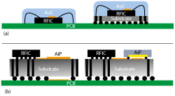
Figure 1 AoC (a) and AiP (b) integration schemes.
The underexploited millimeter wave (mmWave) frequency range (30 to 300 GHz) was restricted to niche applications, such as spectroscopy and military radar, until the late 70s. The front-end complexity and the need for nonstandard fabrication techniques kept the cost of mmWave modules out of reach of high volume and consumer markets. Since the early 80s, major advances have been demonstrated by R&D institutes1 and achieved in the semiconductor industry, opening new horizons for a wide range of applications: high data rate communications, automotive radar, airborne and missile tracking systems, space spectrometry and imaging. Global revenue of the mmWave components market was estimated to be around $116 million in 2013 and is expected to reach $1.1 billion by 2018, which would be a compound annual growth rate (CAGR) of about 59 percent.2 While this can be viewed by the industry as a great economic opportunity, the emerging applications are bringing specific challenges in terms of electrical performance, compactness, integration possibilities and system reliability. This article focuses on short to mid-range communication devices that illustrate some of the technical challenges related to the integration of wireless transceivers and their coexistence with other components. The short wavelengths at mmWave frequencies can be seen as an opportunity to integrate passive components whose typical dimensions become compatible with standard electronic packages. For some of the applications, bulky elements such as waveguides, connectors, nonplanar filters and large antenna arrays still slow the progress towards fully integrated and miniaturized systems. In the case of short-range, 60 GHz communications, portable devices are expected to be the main market driver for the coming decade — hence the need for fully integrated, compact and yet high performance transceivers. Regarding antennas, the miniaturization process is limited by the fundamental relation between the radiator’s area and the achievable gain; this is often seen as the bottleneck for full integration of wireless transceivers.
INTEGRATING TRANSCEIVERS WITH ANTENNAS
The antenna-on-chip (AoC) approach consists of integrating the radiating elements directly into the back-end stack of an RFIC chip, whether it is fabricated in CMOS, BiCMOS or III-V technology (see Figure 1a). The main advantages of this solution lie in the absence of any RF interconnect and the co-integration of all RF and baseband functions on a single module a few square millimeters in size. However, for silicon-based AoCs, the high permittivity (εr = 11.7 to 11.9) and low resistivity (þ ~ 10 Ω∙cm) of the substrate severely degrade the matching bandwidth and radiation efficiency. Still, the properties of AoC antennas can be improved by locally modifying the properties of the substrate. This can be done, for example, by etching an air cavity below the radiating element or by realizing a suspended membrane. The presence of an air layer in both cases minimizes the dielectric loss and lowers the effective permittivity. Other innovative solutions include the local modification of the silicon substrate resistivity using an ion-implantation process or the above-IC integration of coupled radiating elements.

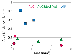
Figure 2 Typical area efficiency for integrated antennas.
In an antenna-in-package (AiP) integration approach, the antenna is realized on a separate substrate, independent of the RFIC chip (see Figure 1b). This substrate can either be specifically dedicated to the radiating element and its feeding lines or play the role of a package for transceiver assembly and heterogeneous integration. For this reason, AiP designs play a key role in a 3D integration scenario for mmWave transceivers, while giving an additional degree of freedom with the choice of low permittivity and/or high resistivity substrates. Moreover, the area allowed for the antenna stage can be greater than what is allowed by AoCs. Consequently, a valid base of comparison of integrated antenna performance should take into account the allocated area, and we can define a new figure of merit normalizing the realized gain (in linear scale) per unit area. Figure 2 plots a literature survey of 60 GHz integrated antennas, showing that the gain of AiPs is two to four times higher than AoCs, due to the use of low loss substrates instead of CMOS-grade silicon.
MAINSTREAM mmWAVE PACKAGING
The selection of a given technology for the integration of wireless transceivers is a trade-off between several constraints: electrical performance, thermo-mechanical reliability, compactness, manufacturability and cost. Inherited from the well established and mature PCB technology, today’s high density interconnect (HDI) design rules allow lines and gaps below 40 µm and micro-via formation with diameters under 100 µm, which are compatible with the requirements of mmWave integration. Moreover, the new generation of multi-layer organic (MLO) packages uses high quality dielectrics in both thin and thick film configurations. As a result, standard FR-4 cores and redistribution-layer laminates are progressively being replaced with low loss dielectrics such as the RO family and liquid crystal polymers (LCP). As one example, STMicroelectronics developed a 60 GHz, HDI, organic package using a technology based on a symmetric stack-up with an RO4003C core.3
In the same context, ceramic packages were introduced about two decades ago to meet the needs of critical systems, thanks to their properties of chemical stability, mechanical reliability and hermetic assembly. Ceramic processing allows the creation of a variety of via and cavity structures as well as the assembly of external capacitors and inductors. The vertical resolution for standard multilayer ceramic packages is around 50 µm. The two main multilayer ceramic processes currently used are low temperature co-fired ceramic (LTCC) and high temperature co-fired ceramic (HTCC), with respective maximal co-firing temperatures of about 900°C and 1600°C. While the HTCC process provides a great physical stability to the package, only high melting point metals such as tungsten (Tf = 3422°C) and molybdenum (Tf = 2623°C) can be used for routing in the internal layers. Unfortunately, these metals exhibit relatively low conductivity (8.9 × 10⁶ and 18.7 × 10⁶ S/m, respectively) compared to LTCC’s copper, titanium/gold alloy or silver metallization, which have lower conductive losses at high frequencies. Several convincing contributions from the industry can be found in the literature, such as IBM’s 60 GHz LTCC module along with an MLO package (RO4000 and LCP).4,5
One of the fastest growing packaging technologies, embedded wafer-level ball grid array (eWLB) is a wafer-level packaging approach that combines advanced redistribution layer processing with a wafer-to-molding transfer technique. The molding polymer plays a double role in protecting the ICs and supporting fan-out routing. The eWLB processes (including under-bump metallization) are inherited from silicon micro-fabrication lines. Thanks to the use of low stress molding polymers, eWLB packages can be suitable for large packages featuring antenna arrays, while ensuring a line/space critical dimension around 15 µm. Several demonstrations of mmWave packages with integrated antennas can be found in the literature, with an emphasis on radar applications as demonstrated by Linz University and DICE GmbH.6,7 This recent technology offers promising perspectives for 3D integration thanks to package-on-package (PoP) assembly possibilities using through-package interconnects.
Today’s silicon back-end lines provide a large panel of micro-fabrication techniques to realize systems-in-package (SiP), such as micromachining, photolithography, ion and laser etching as well as a large panel of deposition and lamination techniques. Standard silicon processes can easily achieve micron resolutions and meet the requirements of mmWave and even sub-THz systems. In the last five years, organic and silicon interposer packages have been popularized by ASIC and memory applications, but recent trends in heterogeneous integration show more demonstrations of RF functionality as well as the introduction of glass as a potential candidate for high frequency applications.
SILICON vs. GLASS INTERPOSERS
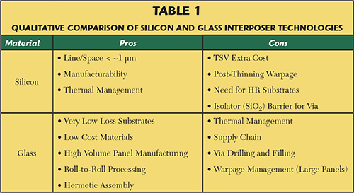
As stated before, silicon micro-fabrication is particularly suitable for mmWave applications thanks to the unequaled resolutions with mature and standard back-end processes. Silicon packages provide excellent thermal conductivity (σ~ 150 W∙m-1∙K-1 at 25°C) compared to ceramics (σ< 20 W∙m-1∙K-1) and PCB materials (σ< 1 W∙m-1∙K-1), important in a typical scenario where an external power amplifier is assembled with the transceiver chip.

Recent years have produced increasing interest for 2.5D and 3D glass interposers and the new integration opportunities they offer. Glass substrates are known to have excellent dielectric properties with a low dielectric constant (εr ~ 4 to 6, depending on the composition and process) and a low loss tangent, which make them good candidates for RF packaging and passives integration. Table 1 compares glass and silicon interposers. The replacement of wafers with large panels favors mass production, while significant advances have been made in through-glass-via (TGV) drilling and filling as well as redistribution layer (RDL) processing. Today’s glass interposer task force is driven by manufacturers and suppliers such as Asahi, Corning Glass and 3D Glass Solutions as well as academic research organizations such as Georgia Tech, which leads an international interposer consortium. However, the supply chain for glass panels and processing equipment is not as well defined as for silicon, organic, ceramic and eWLB technologies. 2.5D/3D glass interposer technology is more likely to reach full maturity with the next generation of 3D integrated devices; currently, it is adequate for niche applications such as high performance computing and datacenters, where there are less concerns about cost.8

Figure 3 Schematic cross section of the 60 GHz module (a) and microphotograph of the silicon interposer chip (b).
The first fully functional interposer package developed at CEA-Leti is based on a high resistivity (ρ > 1 kΩ∙cm), 120 µm thick silicon substrate with two front-side and one back-side copper redistribution layers. Each side of the interposer carries an under-bump metallization used, respectively, for RFIC flip-chip (using copper pillars or micro-bumps) and package assembly on the main PCB board using ball grid array (BGA) solder balls.9 The two sides of the interposer chip are interfaced using copper-filled through-silicon-via (TSV) interconnects with 60 µm diameter (an aspect ratio of 2:1). The total area of the interposer is 6.5 mm × 6.5 mm, making it the most compact 60 GHz transceiver with integrated antennas reported to date. Figure 3a shows an unscaled cross section of the module with the interposer, RFIC chip and the molding polymer used to ensure the integrity of the assembly. The 60 GHz RFIC transceiver is fabricated using 65 nm CMOS technology.10 Two folded dipole antennas (for transmit and receive) are hosted on the upper front-side RDL level. A guard ring made of a copper strip and an array of TSVs is used to mitigate surface wave coupling between the two cavity-backed antennas (see Figure 3b).

Figure 4 Schematic cross section (a) and SEM view (b) of a TSV-Last.

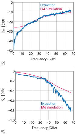
Figure 5 Reflection (a) and transmission (b) of a 50 Ω terminated TSV transition in the GSG configuration.
This module is a typical demonstration of a 2.5D integration scheme, where the RFIC is assembled on top of the interposer and placed with an offset from the antennas. The vertical interconnects are realized using Leti’s custom TSV Via-Last process. Figure 4 shows a cross section and SEM image of a TSV. While the main function of TSV interconnects in the transceiver is to drive low frequency and baseband signals, the test vehicle included additional test features to investigate their suitability for mmWave through-package routing and back-side antenna feeding. The TSV electrical performance has been investigated using RF probe measurement and proper de-embedding techniques to extract the broadband response of a single GSG transition across DC to 67 GHz.11 The transitions demonstrated about 0.6 dB insertion loss at 60 GHz, with the impedance mismatch to the 50 Ω terminations as a major contributor, i.e., 0.46 dB (see Figure 5). In addition to broadband characterization, baseband signal integrity has been investigated using an inverse Fourier transform of the frequency domain response. The transient eye diagram analysis with a 5 Gbps pseudo-random binary sequence (PRBS) demonstrated an eye opening of 96 percent.
ONGOING DEVELOPMENT
The ongoing research at Leti aims to create a new generation of mmWave interposer packages with enhanced electrical and mechanical properties and reasonable cost and manufacturability, compared to other competing technologies. The new module, currently undergoing layout and prefabrication analysis, keeps the same overall thickness as the first demonstrator; however, the total area is reduced by about 33 percent (from 6.5 mm × 6.5 mm to 5.3 mm × 5.3 mm) thanks to an integrated high impedance surface (HIS) reflector design (see Figure 6a).12 Two evolutions are being evaluated to enhance antenna performance, as shown in Figure 6b. The first involves laminating a molding polymer on top of the interposer and processing metal parasitic patches to enhance the bandwidth. The second aims to provide mid-range communication capabilities (around 10 m) with an external dielectric lens. In this case, the targeted gain at 60 GHz is 15 dBi. The proposed lens designs are based on hemispherical and parabolic geometries using PA6-class machined plastics (εr = 4.3). Two of the four designs, with 6 mm and 1 cm diameter hemispherical lenses, have been experimentally validated. The first measurement used an open WR15 waveguide feed and demonstrated gains of 12 to 16 dBi across 57 to 66 GHz. Following a system-level validation workflow, the lenses have been co-integrated with a 60 GHz QFN transceiver module13 and demonstrated a range improvement by factors of four for one transmit lens and 7.5 for transmit and receive lenses.
ACKNOWLEDGMENT
This work is partially supported by the French Ministry of Defense, DGA (Direction Générale de l’Armement) and the Carnot Institut program under the “RF INTERPOSER” project.

Figure 6 Simplified layout of the 3D interposer, courtesy of A. Moknache (a) and new 3D integration schemes with HIS-based antennas (b).
References
- L. Dussopt, Y. Lamy, J. Lantéri, H. Sibuet, B. Reig, C. Dehos, P. Vincent, S. Joblot, P. Bar and J.F. Carpentier, “Silicon Interposer with Integrated Antenna Array for mmW Short Range Communications,” IEEE International Microwave Symposium, Montreal, Canada, 2012.
- Research and Markets, “Millimeter Wave Market — By Technology, Components, Products and Applications,” www.researchandmarkets.com.
- R. Pilard, D. Titz, F. Gianesello, P. Calascibetta, J. Riviere, J. Lopez, R. Coffy, E. Saugier, A. Poulain, F. Ferrero, C. Luxey, P. Brachat, G. Jacquemod and D. Gloria, “HDI Organic Technology Integrating Built-In Antennas Dedicated to 60 GHz SiP Solution,” IEEE Antennas and Propagation Society International Symposium (APSURSI), Chicago, Ill., 2012.
- D.G. Kam, D. Liu, A. Natarajan, S.K. Reynolds and B.A. Floyd, “Organic Packages with Embedded Phased-Array Antennas for 60 GHz Wireless Chipsets,” IEEE Transactions on Components, Packaging and Manufacturing Technology, Vol. 1, No. 11, p. 1806, 2011.
- D.G. Kam, D. Liu, A. Natarajan, S. Reynolds and B. Floyd, “Low-Cost Antenna-in-Package Solutions for 60 GHz Phased-Array Systems,” IEEE 19th Conference on Electrical Performance of Electronic Packaging and Systems (EPEPS), Austin, Texas, 2010.
- A. Fischer, Z. Tong, A. Hamidipour, L. Maurer and A. Stelzer, “A 77 GHz Antenna in Package,” 41st European Microwave Conference (EuMC), 2011.
- M. Wojnowski, C. Wagner, R. Lachner, J. Böck, G. Sommer and K. Pressel, “A 77 GHz SiGe Single-Chip Four-Channel Transceiver Module with Integrated Antennas in Embedded Wafer-Level BGA Package,” 62nd ECTC, San Diego, Calif., 2012.
- 3DInCites, “Glass vs. Silicon Interposers for 2.5D and 3D IC Applications,” www.3dincites.com.
- C. Ferrandon, A. Jouve, S. Joblot, Y. Lamy, A. Schreiner, P. Montmeat, M. Pellat, M. Argoud, F. Fournel, G. Simon and S. Cheramy, “Innovative Wafer-Level Encapsulation & Underfill Material for Silicon Interposer Application,” IEEE Electronic Components and Technology Conference (ECTC), Las Vegas, Nev., 2013.
- A. Siligaris et al., “A 65-nm CMOS Fully Integrated Transceiver Module for 60 GHz Wireless HD Applications,” IEEE Journal of Solid-State Circuits, Vol. 46, No. 12, pp. 3005–3017, 2011.
- T. Lacrevaz, C. Bermond, O. El Bouayadi, G. Houzet, P. Artillan, Y. Lamy, K. Dieng and B. Flechet, “Electrical Broadband Characterization Method of Dielectric Molding in 3-D IC and Results,” IEEE Transactions on Components, Packaging and Manufacturing Technology, Vol. 4, No. 9, pp. 1515–1522, 2014.
- O. El Bouayadi, Y. Lamy and D. Laurent, “A High-Impedance Surface Antenna On Silicon Interposer for 3D Integrated mmW Transceivers,” European Microwave Week, Rome, Italy, 2014.
- J. Zevallos Luna, L. Dussopt and A. Siligaris, “Packaged Transceiver with On-Chip Integrated Antenna and Planar Discrete Lens for UWB Millimeter-Wave Communications,” IEEE International Conference on Ultra-Wideband, Paris, France, 2014.
