
Power supply noise may create timing failures in FPGA core logic [1] and may increase jitter in input/output (I/O) blocks [2]. Existing power integrity analysis tools use extracted S-parameter models of the power distribution network (PDN) on die, package, and PCB to evaluate the power supply noise seen by active circuits [3]. These tools work well in a custom integrated circuit design process where designers have full access to the schematic and layout design files of the die, package, and PCB. However, in an FPGA system design process there is no access to the schematic and layout design files of the FPGA die and FPGA package [4], limiting the efficiency of power integrity analysis and increasing the chances of power supply noise induced failures. Simulation of power integrity in FPGA using S-parameter models has been reported in [5] where authors from Xilinx and Keysight created a test bench simulation in Keysight ADS software tool using S-parameter models of a Xilinx 7 series FPGA device package and an S-parameter model of a printed circuit board.
This article presents a novel method for power integrity analysis in FPGA systems by configuring the FPGA to function as a vector network analyzer (VNA) test instrument for its own power distribution network (PDN). This embedded VNA measures the impedance frequency profile of the PDN as seen by the logic circuits of the FPGA fabric and extracts a complete S-parameter model of the power distribution network of the FPGA system that includes the PDN elements on the FPGA die, FPGA package, and PCB. The S-parameter model can be then used in circuit simulation tools to evaluate the power supply noise in the FPGA core logic and the timing jitter in the FPGA I/O data links.
Implementation
There are two basic types of network analyzers: scalar network analyzer (SNA) that measures magnitude only and vector network analyzer (VNA) that measures both magnitude and phase. S-parameter models contain both magnitude and phase information, so, in order to extract an S-parameter model of the FPGA PDN, the embedded test instrument has to be a VNA type.
Commercial test bench VNAs are designed to interface with the measured network in a controlled characteristic impedance transmission line environment through coaxial cables and connectors. The transmission line environment makes it more convenient to measure the transmitted and reflected waves at each port. An FPGA embedded VNA has the interface with the measured network where the core logic or I/O blocks connect to their power supply rails on the die. In static mode, when there is no switching activity, logic core and I/O blocks are high impedance elements connected to the power supply rails. This functionality mode makes it possible to set VNA ports in “open circuit” mode, thus, for on-die PDN VNAs it is more convenient to measure the Z-parameters matrix and then convert it into S-parameters matrix. The parasitic effects of “open” mode become included in the PDN model.
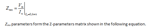
Figure 1 shows a top level block diagram of a multi-port VNA instrument implemented in an FPGA. In this diagram the VNA has one measurement port connected to the core logic power domain, VNA P1, and additional measurement ports connected to each I/O bank VNA P2, VNA P3 … VNA P8. All measurement ports are controlled from a frequency generator and data processing block, which is controlled through a serial data link from a software application running on a computer.
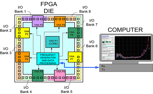
Figure 1 – Top Level Block Diagram of an FPGA Embedded Vector Network Analyzer (VNA)
Activating port n generates a sinusoidal current  through the PDN. The other ports are in high impedance “open” mode. This sinusoidal current generates sinusoidal voltage variation at port
  and sinusoidal voltage variations
  at the other ports if there is coupling in the PDN. All VNA ports measure the magnitude and phase of the voltage variation of their corresponding power domain.
  parameters are calculated by dividing
VNA Port Structure
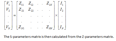
Each VNA measurement port in this design includes a transmitter and a receiver as shown in Figure 2.
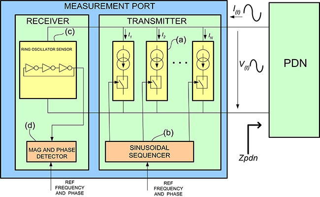
Figure 2 – Block Diagram of a VNA Measurement Port
The transmitter generates a sinusoidal current through the power distribution network by sequentially activating and de-activating a variable number of constant current load blocks (a). Each constant current block is made of FPGA logic blocks or FPGA I/O blocks by sequencing multiple transient switching currents so that they superimpose to an overall constant current pulled from the positive supply rail and pushed into the negative supply rail. The activation of constant current loads is controlled by a sinusoidal sequencer (b). The frequency of the sinusoidal current is controlled from a programmable frequency generator configured in the FPGA.
The sinusoidal current from transmitter, I(t) generates a sinusoidal voltage variation, V(t), on the power supply domain following formula V(t) = I(t)*Zpdn, where Zpdn is the impedance of the power distribution network. Figure 3 shows an example of sinusoidal variation of the FPGA supply voltage generated by a VNA transmitter port.
Figure 3 – Sinusoidal variation of FPGA core logic voltage supply generated by a VNA transmitter and measured on the board
The upper trace represents the FPGA power supply voltage measured on the board and the lower trace represents a trigger signal generated in the VNA transmitter port.
The receiver includes a ring oscillator (c) powered from the same power domain as the transmitter. This ring oscillator sees the sinusoidal voltage variation V(t) as amplitude modulation of its power supply. The frequency of oscillation in ring oscillators is proportional to the delay of each stage of the ring oscillator chain. The delay through each stage increases when power supply voltage decreases and decreases when power supply voltage increases. Therefore, the sinusoidal variation of the power supply voltage, V(t), modulates the frequency of the ring oscillator as shown in the figure 4.
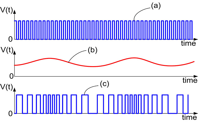
Figure 4 – Ring oscillator frequency modulation caused by power supply voltage variation
If the power supply voltage is constant the ring oscillator oscillates at a constant frequency as shown by trace (a). When the sinusoidal power supply current load is active, and the power supply voltage varies as shown by trace (b), the frequency of the ring oscillator is modulated following a sinusoidal variation as shown in trace (c).
The magnitude and phase detector block, (d) in Figure 2, measures the modulation magnitude and phase of the ring oscillator. The magnitude of the impedance parameter is calculated as
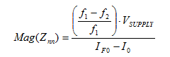
where Znn represents the impedance parameter of the power distribution network port n when port n transmits and all the other ports are “open”, f1 is the frequency measured with the sinusoidal power supply current load not active, f2 is the frequency measured with the sinusoidal power supply current load active, VSUPPLY is the nominal value of the power supply voltage supplied by the power distribution network, IF0 is the current consumption of the programmable logic device with the frequency of the sinusoidal power supply current load set to zero, and I0 is the current consumption of the programmable logic device with the sinusoidal power supply current load not active. The phase is measured by a phase detector having as reference the phase of the transmitted sinusoidal signal. When a different VNA port generates the sinusoidal current, the measured impedance represents Zmn parameter, where m is the measurement port and n is the transmitter port.
The Z-parameters matrix is then converted into S-parameters matrix. S-parameters are dependent on the source and load impedances, so the conversion is done for an arbitrary reference impedance ZREF. The conversion uses algebraic computations derived using fundamental laws of electric circuit analysis. Here is an example conversion of a two port Z-parameters matrix to S-parameters matrix:

For PDN models ZREF value is typically 0.1 Ohms, but other values can be used too. The S-parameters matrix is then documented in an S-parameter model using the Touchstone format.
Measurements on a Test Vehicle Board
Figure 5 shows an example of S-parameter model measured in a Spartan 3 FPGA test vehicle board using a two port VNA IP. Port 1 measures the VCCINT core power supply and port 2 measures one I/O bank, VCCIO, power supply:
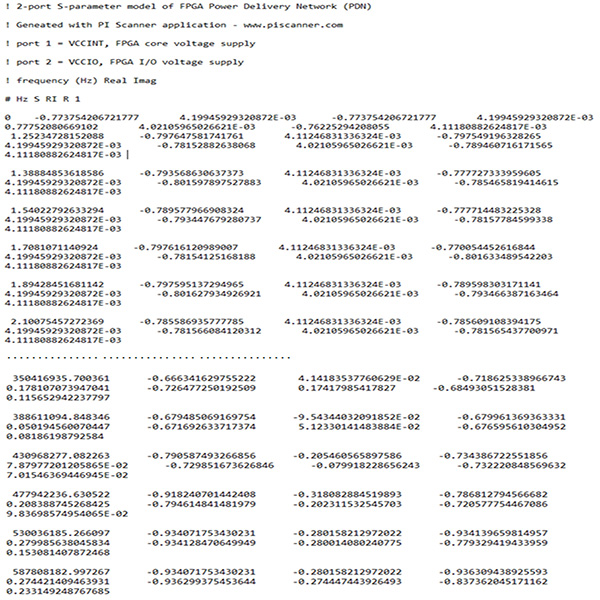
Figure 5 – S-parameter model of a Xilinx Spartan 3 FPGA measured on a test vehicle board
The example in Figure 5 shows the beginning and the end of the S-parameter model. The minimum frequency is 0 Hz and the maximum frequency is 587 MHz. To increase the measurement frequency all the way to the maximum clock frequency of the FPGA, in this case 587MHz, the transmitter sinusoidal current becomes gradually “distorted” to the point where it is a square wave at 587MHz. One advantage of obtaining the S-parameter model from Z-parameters matrix is that the 0 Hz values are directly obtained from measurements instead of extrapolating from higher frequency measurements like in transmitted/reflected wave measurements.
This S-parameter model can be further used in circuit simulator CAD tools for power integrity and signal integrity simulations on serial data links connected to the FPGA. Figure 6 shows an example of the above S-parameter model used in a simple Keysight ADS circuit simulation testbench:
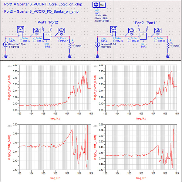
Figure 6 – Simulation of a simple circuit using the Xilinx Spartan 3 PDN extracted S-parameter model
The PDN impedance magnitude can be displayed directly in the measurement application software, like in Figure 7 example that uses the VNA IP and PI Scanner tool from http://www.piscanner.com:
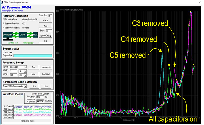
Figure 7 – Measurement of FPGA PDN impedance with the embedded VNA and PI Scanner software application
This measurement has been done on a test vehicle board using a Xilinx Spartan 3 FPGA, shown in Figure 8.
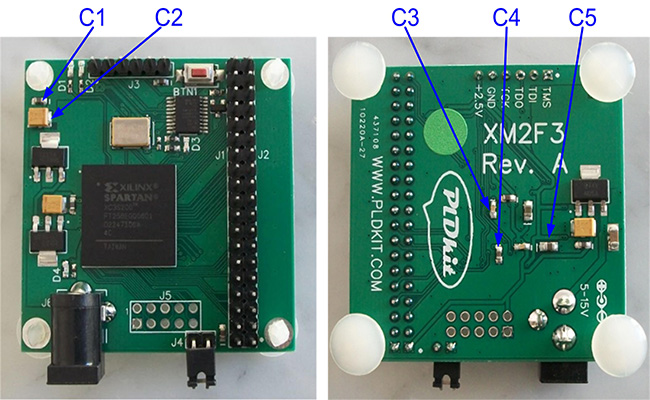
Figure 8 – Location of core logic supply decoupling capacitors on the Xilinx Spartan 3 FPGA test vehicle board
Decoupling capacitors C3 (10nF), C4 (100nF), and C5 (10uF) have been removed one at a time and the PDN impedance re-measured.
Advantages
- Probing ports are right at the logic gates power supply rails inside the FPGA die, so measurement results reflect exactly the impedance that the electric circuits of FPGA fabric see when looking into the power distribution network (PDN)
- Measurements cover the entire system-level PDN from the FPGA die, through package, printed circuit board (PCB), all the way to the voltage regulator module (VRM) and including the VRM
- Measurements include the impedance and transfer function of on-die voltage regulators implemented in some FPGAs
- This method can be used in 3D-IC, stacked die, and multi-die FPGAs and the measurements cover the PDN path on silicon interposers and other stacked silicon interconnects (SSI) and the noise coupling between different FPGA power domains
Future Work
- Test this method on a large high performance FPGA like a Xilinx Virtex UltraScale+ or an Altera/Intel Stratix10 device.
- Develop a method to de-embed the FPGA die+package S-parameter model from the measured overall die+package+PCB model. The de-embedded model can be further used for power integrity and signal integrity simulations in new projects before PCB fabrication.
References
[1] Hui Lee Teng, Shishuang Sun, Man On Wong; Boyle, P.; Chee Seong Fong, “PDN in FPGA may generate timing failures”, 2010 International Conference on Applications of Electromagnetism and Student Innovation Competition Awards (AEM2C), pp 75 – 79
[2] W.L. Lee, M.S.Chin, W.S.Choo, C.K. Chee Intel Corporation, "Predictive Method for Simultaneous Switching Output Jitter of DDR for FPGA", 37th International Electronic Manufacturing Technology Conference, Penang, Malaysia, 2016
[3] Raymond Y. Chen, Sam Chitwood, "Fundamentals of S-Parameter Parameter Modeling for Power Distribution Modeling for Power Distribution System (PDS) and SSO Analysis", IBIS Summit June 14, 2005 Anaheim, CA
[4] Jongmin Kim, In-Woo Lee, Sungjun Kim, So-Young Kim, Wansoo Nah, "Novel Extraction Method for Unknown Chip PDN Using De-Embedding Technique", The Journal of Korean Institute of Electromagnetic Engineering and Science, 2013 Jun, pp 633∼643
[5] Hany Fahmy and Colin Warwick of Agilent Technologies, Inc. and Jack Carrel, Ray Anderson, Harry Fu, and Romi Mayder of Xilinx, Inc., "Simulating FPGA Power Integrity Using S-Parameter Models", Xilinx white paper WP (v1.0), January, 2012