
A schematic tells us what components are used in the circuit and how they connect. It tells us nothing about signal integrity, power integrity, or EMI. These important properties live in the ideal wires connecting each component and in the white space of the schematic. All the important design information about high-speed performance is hidden and can only be seen in the mind of the engineer. This is one of the most important lessons engineers can learn when they start out designing circuits and boards.
In the mixed undergraduate/graduate course taught at the University of Colorado, Boulder, “Practical Printed Circuit Board Design and Manufacture,” students learn this important lesson in their first board design project.
A Simple Board Project
The circuit design is very simple. A 5 V power plug supplies power to the board. It drives a 555 timer designed for a 10 kHz square wafer with a 90% duty cycle. A simple LDO converts the 5 V into a 3.3 V rail which powers a hex inverter chip. One of the inverters has its input tied high so it is always producing a low. Four other drivers have inputs connected to the output of the 555 timer so they switch with the square wave, but invert the 90% duty cycle to a 10% on duty cycle. The simple schematic is shown in Figure 1.

One of these switching signals makes its way to a test point where the signal can be measured. This is used to trigger an oscilloscope so we have a reference for the switching edge. When the scope is set for 50 Ohms input, the current draw is 3.3 V/50 Ohms = 66 mA. When a 10x probe is used, the load impedance on the output of the inverter is much higher than 50 Ohms, and less than 10 mA switches on each edge.
The other three switching signals drive 50 Ohm resistors in series with red LEDs. The current through each LED is estimated as about (3.3 V – 1.8 V )/50 Ohms = 30 mA. This means when the hex inverter chip switches, as much as 100 mA will flow on each edge and can be as much as 150 mA when 50 Ohms is used in the scope input.
Translating Schematic to Layout
In the first class exercise, this schematic is translated into a 2-layer circuit board layout in two forms. On the first day of class, students are given the board with the parts placed in specific locations. Their first assignment is to route the traces taking into consideration ONLY the connectivity. This uses all the information in the schematic, implemented however they want. Since few students come into this class with experience in best design practices, most of the boards are routed with signal, power, and ground traces all over the place, going back and forth between the two layers.
Their boards are sent out to fab and students assemble and test these boards. In parallel, another version of this board, a “golden board,” is fabricated that uses a ground plane and all signals and power traces routed on the top layer.
An example of these two different boards are shown in Figure 2.
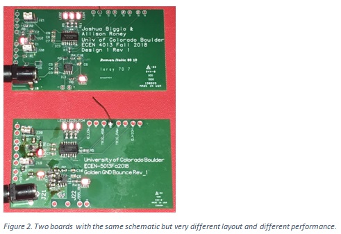
It should be noted that each board came from exactly the same schematic. The difference is that the golden board layout was based on best design practices while the student board was not. They both have a 10 kHz, 90% duty cycle square wave, with a hex inverter switching about 100 mA on each edge. These two boards have a radically different noise levels.
Measuring Ground Bounce with a Quiet Low Line
We use the hex inverter output pegged low as a sense line to transmit the voltage on the die’s ground rail, compared to the board level ground, through the signal path to a probe point on the edge of the board. We call this sort of pin a “quiet low” pin. This is a very common technique to measure the ground bounce on the ground rail of the die.
This voltage is a direct measure of the noise on the ground rail of the die, which all the other I/O drivers see. The difference in these two boards is the ground bounce noise generated because of the layout of the signals and return paths.
In the student board version, the signal path (between the I/O pin to the test point and their return path from the ground pin of the hex inverter and the ground connection on the edge of the board) makes really big loops. Since these loops overlap, there is a huge mutual inductance between them. When currents switch through one of these loops, as when the I/O switches, the dI/dt generates a large voltage in the quiet signal-return path loop.
This is the most common cause of ground bounce. The more I/Os switch simultaneously, each of their dI/dt’s generating induced voltage noise in the quiet loop, the larger the ground bounce noise.
Comparing the Measured Ground Bounce
We use the signal coming out of one of the switching hex inverters as the trigger. Figure 3 is an example of the trigger signal and the quiet line on the student board measured with a scope.

This is not a typo or mis-print. The ground bounce voltage, measured on the quiet line, when the four I/Os switch simultaneously really is more than 3 V peak to peak. If you don’t pay attention to the layout, ground bounce can get very large.
To reduce this problem, use a return plane in close proximity to the signal lines. This forces the return currents to flow directly under the signal lines, creating very small signal-return loops, with no overlap between them.
In the golden board, we use a solid ground (return) plane and route all the signal lines on the top layer. There is very little overlap of the signal-return loops. The noise on the quiet line on the golden board compared to the ground bounce on the student board, is shown in Figure 4.
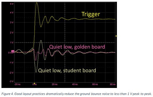
Even though there are no overlapping signal-return path loops on the board, there is still a long, common ground lead in the package. The inductance of this lead will generate some residual ground bounce, which is what we see in this scope measurement. It is less than 1/3 of the noise when layout is not optimized.
Best Design Practice
These boards were designed from exactly the same schematic. They differed only in the layout. Nowhere on the schematic is information about where noise might come from. It is hiding in the white space between the components.
This example illustrates one of the most important best design practices: keep a continuous return path under the signal lines using a solid return plane. If you don’t use a continuous return path, it doesn’t mean your design won’t work, it just means you will have more ground bounce noise generated. Sometimes this noise is enough to kill your product.