
GDDR5 has emerged as a leading DRAM interface for applications requiring high system bandwidth like graphic cards, game consoles, and high-performance compute systems. However, the requirements of newer applications drive even higher memory bandwidth. The paper discusses the development of GDDR6 as a lower-risk and more cost-effective solution as compared to other high-bandwidth memory solutions. We further introduce GDDR6 as offering a 2x increase in per-pin bandwidth over GDDR5, while maintaining compatibility with the established GDDR5 ecosystem. Circuit and channel performance scaling will be discussed and validated through measurement to demonstrate the potential for scaling GDDR6 to 16Gb/s.
GDDR5 has been an enabler of high performance applications for nearly 10 years. While the first devices were introduced at a data rate of 6 Gb/s/pin [1], today, cards reaching 8 Gb/s/pin are readily available in the marketplace. Yet, even the fastest GDDR5 claimed is only running at 9 Gb/s/pin [2, which is barely exceeding the speed of parts already commercially available. Thus, as successful as GDDR5 has been, this apparent slow-down in bandwidth scaling needed to be addressed. To preempt the inevitable gap between market bandwidth demands and available memory component performance, the industry has pursued two parallel paths.
One approach has been to develop a completely new memory architecture, coincidently named high bandwidth memory (HBM) [3]. With the understanding that memory interface performance is limited primarily by the slower DRAM transistor process, as well as the chip-to-chip interconnect, HBM chose to completely redefine the problem by adopting an extremely wide (many wires) interface, thus allowing the DRAM input/output (I/O) circuitry to operate well within the DRAM process capabilities. That redefinition, however, requires a substantial enhancement in the supporting technologies, namely the reliance on silicon interposer and through-silicon-via (TSV) technologies to couple the GPU/ASIC with the DRAM.
HBM, as it has been defined, consists of a TSV-interconnected stack of DRAMs resting on a logic buffer die, which communicates with the GPU/ASIC across a fine-pitched Si interposer-based channel at relatively low per-pin data rates. While the HBM architecture offers many advantages, its complexity (in terms of testability, stability, durability and overall cost) have limited its adoption to only the highest-tier applications.
In parallel with the development of HBM, the more evolutionary path of the GDDR family of DRAMs has continued to scale in performance, offering a more cost-effective and flexible alternative. Without redefining the system, GDDR5X directly addressed the key bandwidth limiters through internal data path and clocking enhancements [4], thus providing for less risky adoption in more cost-sensitive applications (gaming, etc.). GDDR5X is currently found in the marketplace reaching per-pin data rates of up to 11.4 Gb/s [5].
Even as GDDR5X continues to make incremental improvements, the next natural step on the GDDR path was to develop a GDDR6 standard capable of supporting per-pin data rates doubling GDDR5. Presently the official GDDR6 JEDEC standard covers a range from 12 to 14Gb/s, but in this paper, we will demonstrate GDDR6 scalability to at least 16Gb/s/pin. The remainder of the paper is divided into three primary sections: silicon changes (e.g., circuit and architecture) and channel enhancements required to support scaling the single-ended GDDR interface all the way to 16Gb/s, along with performance measurements of Micron’s first 8Gb, 16Gb/s/pin GDDR6 offering.
Silicon Changes
An image of Micron’s first GDDR6 die is shown in Figure 1. While circuit and architectural changes were needed to achieve the new bandwidth target, a primary goal of the GDDR6 component definition was to stay close to the evolutionary path, and thus take advantage of the advanced GDDR5 and GDDR5X infrastructure, including established packaging, handling, and testing methods. As a result, external features like the general command protocol have been held over from the previous standards.

Figure 1: Die photo of Micron’s first 8Gb, 16Gb/s-capable GDDR6 offering
The most prominent new feature, in terms of system application, has been the added support for dual-channel (2 x16) operation. Another change, visible to the system, is support for stronger on-die termination and output driver pull-up strength of 48Ω. While the output driver remains somewhat asymmetric (60Ω/40Ω or 48Ω/40Ω), this support for 48Ω improves signal symmetry, while providing a better match to the typical characteristic impedance of the package + printed circuit board (PCB) channel for enhanced signal integrity.
Aside from these changes, and some specification extensions related to phase locked loop (PLL) operation and clocking flexibility, GDDR6 speeds are enabled through the accumulation of several incremental improvements over the GDDR generations. Data bus inversion (DBI) was introduced as early as GDDR4, and has continued to prove effective at mitigating simultaneous switching output (SSO) noise while lowering signaling power [6]. Decision feedback equalization (DFE) for channel impairment compensation, PLL for jitter filtering, regulated voltage supplies to minimize power supply induced jitter (PSIJ) in the high-speed write clock (WCK) distribution were all included in early GDDR5 designs [1]. Output driver boosting (similar to pre-emphasis) was incorporated into GDDR5 to open the data eye as speeds continued to push, while at the same time, innovative internal modes of operation, like frequency controlled switching (FCS) of charge pumps, used to set the varied voltage levels throughout the DRAM, proved helpful in reducing internal supply variation for greater stability along the data path [7]. Duty cycle correction and input clock equalization, along with inductive-capacitive (LC) resonant clock tree termination and a more prevalent use of current-mode-logic (CML) circuit design enabled yet higher speeds through reducing jitter in the DRAM clock distribution [2].
To overcome limitations in DRAM array timing, GDDR5X doubled the data prefetch, increasing the number of bits presented to the output driver with each data access. To double the datarate out of the DRAM without increasing the memory system clock frequency, GDDR5X supports both double data rate (DDR) and quad data rate (QDR) modes of operation. A PLL on the DRAM provides a degree of jitter filtering, and at the same time may be used as a WCK frequency multiplier in QDR mode, though the GDDR6 JEDEC specification provides flexibility in PLL usage, supporting high-speed operation without the PLL.
To improve signal integrity when reading data from the memory, tunable de-emphasis was incorporated into the output driver structure; this is a non-trivial design due to the inherent asymmetry in the unbalanced pull-up/pull-down drive strength definition. Further, to guarantee a more robust interface, increasingly complex and accurate training and calibration of the interface timing and voltage margins has become essential [8], and, as needed, GDDR5 and beyond support per-pin de-skew of the data bus. Finally, to ensure that errors are not introduced during chip-to-chip communication, the results of cyclic redundancy check (CRC) calculations are transmitted from DRAM to the GPU/ASIC over an error detect code (EDC) pin at half of the data rate [4,7]. Nearly all of these incremental advances developed or adopted throughout the history of GDDR find their place within the GDDR6 architecture, and in a later section of this paper corresponding benefits will be quantified through characterization of Micron’s GDDR6 silicon.
Channel Enhancements
While the chip-to-chip interconnect consists of several key components, many of which are the responsibility of the system architect, one key channel component which is defined within the JEDEC standard is the ball assignment for the ball grid array (BGA) of the DRAM package. Not only does the ball assignment influence signal integrity within the DRAM package, but it can either facilitate or hinder the routing of the main PCB channel. This is because the relative proximity of signals in the ball grid extends into the PCB through the vertical via transitions to the planar routing layers, which could be 100s of microns deep within the PCB substrate.
The ball grid often represents a compromise between the needed signal integrity of the channel, the spatial requirements of the die physical layer (PHY), the greater die architecture, and cost. The ball grid should limit unwanted signal coupling (crosstalk) in the vertical interconnect, while promoting clean routing of signals, including sufficient and consistent signal return paths to their optimal locations at the silicon interface.

Figure 2: Comparison of the JEDEC-specified BGA ball assignments for GDDR5X and GDDR6 (upper-left quadrant, single-byte only).
Figure 2 compares the upper-left quadrant of the JEDEC-specified GDDR5X and GDDR6 package ball assignments; each of the four quadrants supports a single byte of data lines. While not shown in this format, the transition from GDDR5X to GDDR6 included a slight increase in ball pitch from 0.65mm to 0.75mm. On the other hand, as shown, the newly-defined GDDR6 ballout distributes the high-speed data signal balls over a larger area within the grid by extending into the fourth column from the center of the package (column 2), leading to several advantages. For example, VSS balls are more equally distributed across the ball matrix resulting in better signal returns. Coupling between data lines and the even more critical WCK lines is reduced, as well as coupling between data and EDC pins. The proximity of uni-directional (WCK, EDC, etc.) and bi-directional (DQ, DBI, etc.) signals in the package produces distinct coupling conditions during DRAM read and write operations, and warrants careful analysis.
A qualitative evaluation of the worst-case data ball positions in the GDDR5X and GDDR6 definitions projects that the DQ3 signal in the GDDR5X case will experience far-end crosstalk (FEXT) from DQ0, DQ1, DQ2 and WCK, with even more detrimental near-end crosstalk (NEXT) from the EDC signal. (NEXT is expected to be a greater concern, as much of the FEXT will be mitigated through stripline routing of the high-speed signals.)
In the GDDR6 case, the DQ2 signal experiences FEXT from DQ0, DQ1 and DQ3 and NEXT from EDC. Thus, the high-speed clocks have been spatially separated from the single-ended data lines. Additionally, at least one aggressor has been removed from proximity to the EDC ball, which further increases the robustness of the interface. Of course, this qualitative discussion does not account for the pin assignments at the far (GPU) end of the channel, but the GDDR6 DRAM package ballout at least promotes cleaner channel routing between chips.
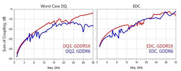
Figure 3: Comparison of crosstalk in GDDR5X and GDDR6 DRAM packages.
Figure 3 adds some data to this qualitative discussion of coupling by presenting the sum of a crosstalk within the DRAM package onto the worst-case DQ lines (left), DQ3 for GDDR5X and DQ2 for GDDR6, along with the sum of all crosstalk onto the EDC lines (right). A DRAM write operation is assumed for both cases, and thus far-end coupling from all signals onto the DQ of interest, with the exception of the EDC, is summed and then combined with the corresponding near-end coupling from the EDC line in the left plot. In the right plot, near-end coupling from all signals onto the EDC line is accumulated.
While the package models were both extracted out to 40GHz, the GDDR5X extraction accounted for half of the physical package, while the GDDR6 extraction only accounted for a quadrant of the package, which may help to explain the apparent differences in “smoothness” of the response curves. It is clear, however, from the left side of Figure 3, that the accumulated coupling onto the worst-case DQ is improved in the GDDR6 package, consistent with our intuition-based comparison of the two ball-outs. The improvement in the EDC response, on the right, may not be as clear, but poses less of a problem as the specification allows for the EDC signal to toggle at half-rate.
As a developer of memory technologies, Micron does not often delve into the world of system architecture and design. Yet, as all high-speed interface designers know, it is difficult to produce an optimized composite channel when developing the distinct component packages and main substrate connectivity in isolation. Thus, to facilitate better DRAM packaging and I/O characteristics, Micron purchased recent “off-the-shelf” high-speed graphics cards to study the typical DRAM to GPU interconnect as a point of reference for channel optimization studies (see Figure 4). Such an approach has greatly increased our modeling confidence, in that our assumptions (channel length, pitch, stack-up, etc.) are justified through commercially available technologies.

Figure 4: Exemplary GPU-to-DRAM channel from an “off-the-shelf” graphics card.

Figure 5: End-to-end channel model producing all simulation results throughout this paper.
That said, none of the simulation results shared in this paper correspond directly to an analyzed graphics card channel. Rather, we have chosen to share results based on simulations couched in distinct, yet reasonable assumptions. Our end-to-end channel model is symmetric, assuming the via transitions below the DRAM package, as well as the DRAM package routing / construction, at both ends of the link, as shown in Figure 5.
As indicated in the figure, the channel is broken into segments to allow for more accurate 3D modeling of the vertical interconnect and package, while the main PCB route is represented by 2D models for flexibility in studying the impact of channel length, data line width, routing pitch, stack-up, etc. Both ends of the channel are terminated, depending on the direction of the signaling operation, through 48Ω or 60Ω to a 1.35V VDDQ supply. The parasitic capacitive loading at the die pad is assumed to be 0.5pF at each end of the channel. While countless transistor-level simulations have been completed for both the output and input paths of the DRAM, all simulation results shown in this paper are based on linear driver modeling to enable rapid, peak distortion analysis (PDA) of worst case pattern conditions [9]. We acknowledge that the unmatched pull-up/pull-down characteristics of the driver cannot be perfectly captured through linear modeling, but we remain confident, based on internal modeling correlation, that this assumption does not significantly alter the results of the paper.
As a goal of this paper is to demonstrate bandwidth scalability in GDDR6, Figure 6 presents the worst-case data eye openings at 14Gb/s and 16Gb/s for the baseline model. It is important to note that the platforms, on which the exemplary channel models were based, were not designed to support 16Gb/s. Thus, the cases shown in Figure 6 potentially push beyond the boundaries of expected performance. Nevertheless, it is observed that with the available DFE functionality incorporated into GDDR6, this channel delivers an open eye at 14Gb/s. At 16Gb/s; however, the received data eye is completely closed, even after equalization.

Figure 6: Baseline channel simulation employing available single-tap DFE, but without any other channel enhancements.
What steps then may be taken to enable 16Gb/s signaling over this basic channel structure (e.g., materials, distance, routing cross-section, etc.)? One option, not incorporated into the model that produced the eyes in Figure 6, is the well-known back drilling of vias to mitigate impedance discontinuities and crosstalk in the vertical interconnects below the component packaging. In the simulation world, it is straightforward to evaluate what impact a process like back drilling would have on overall performance.
Much can be learned from the channel pulse response, as presented in Figure 7. First, a few details. For simplicity, all PDA-based calculations are done on a sample basis, such as x samples per unit interval (UI), rather than on absolute time. While the pulse responses shown are labeled as “volts” and “sample,” final eye measurements are output as absolute voltage and time. All cursors highlighted in red are separated by 1 UI (62.5ps) and are shifted such that the main cursor aligns with the center of the resulting data eye. While only 13 post cursors are shown, several additional cursors are captured and included in all eye closure calculations. The number of cursors must be chosen so as not to ignore perturbations later in the pulse tail. This is particularly true for a high-speed graphics channel, which, being relatively loss-less, may support lingering reflections resulting from imperfect channel termination, as well as other discontinuities.

Figure 7: Pulse response comparison of the channel without and with via back drilling.
Figure 7 compares the 16Gb/s pulse responses for a common data line with and without back drilling. Qualitatively it is observed that back drilling positively impacts the channel response in a variety of ways. First it increases the main cursor value (amplitude), while reducing the first three post cursors significantly. Further, it greatly reduces the magnitude of the signal reflection dispersed over post cursors 8-13. Based on the superposition of the pre-cursor and first 13 post-cursors alone, PDA projects vertical eye openings of 428.16mV and 269.65mV with and without back drilling, respectively. While one might expect 269.65mV to provide sufficient margin, in the presence of crosstalk the closed data eye shown on the right side of Figure 5 is not necessarily surprising, even with DFE.