Traces on PCBs are often routed between parallel planes. What can be simpler than that? Well, the fact that it is a three-conductor structure that supports propagation of transverse electromagnetic (TEM) waves as well as waves of the parallel plate waveguide (PPW) –superposition of radial or plane waves—complicates things. TEM waves are used to transmit the signal between components while PPW waves are used to deliver power to the components. Both waves are useful, but they have to be separated. For instance, if we launch a TEM wave into a trace with ideal equipotentiality of the parallel planes, we can observe the wave propagating strictly along the traces as in Figure 1 (click on graphic to see animation).
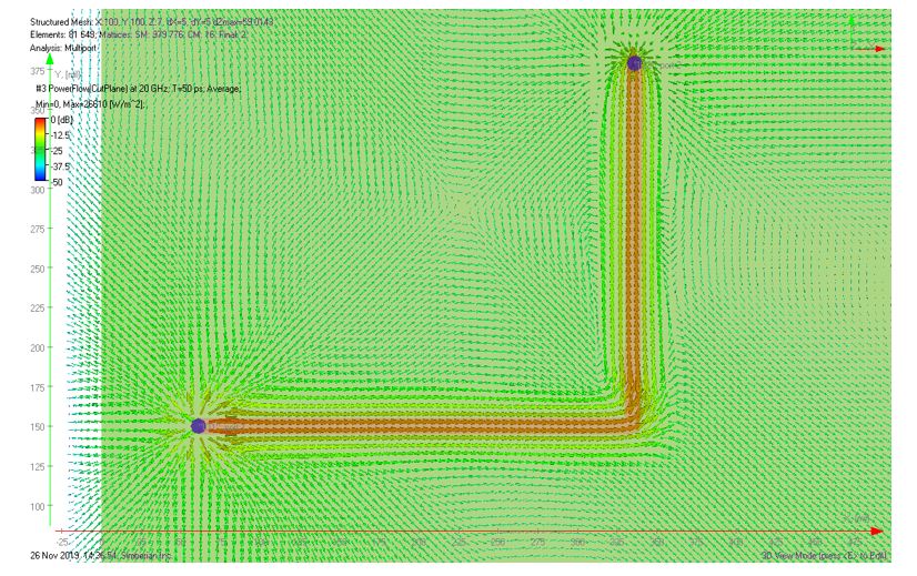
Figure 1. Power flow density in a trace with equipotential planes. The trace segment is excited with a 1 V, 50 Ohm, 20 GHz harmonic source at the bottom left port. Another port is terminated with 50 Ohm. Both ports are via-ports with signal terminal at the trace and reference terminals simultaneously at the top and bottom planes.
What happens if one of the planes is a power plane and the other is a ground plane? Then the equipotentiality cannot be enforced. Figure 2 illustrates what happens with the signal in this case (click on graphic to see animation).
Figure 2. Power flow density in a trace as referenced to one plane. The trace segment is excited with a 1 V, 50 Ohm, 20 GHz harmonic source at the bottom left port. Another port is terminated with 50 Ohm. Both ports are via-ports with signal terminal at the trace and reference terminals at the bottom plane only.
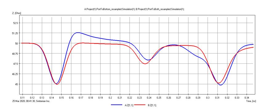
Referencing the excitation to just one of the planes (GND) causes the signal to transform into a useful TEM wave as well as into radial waves of PPW. Waves in PPW are unwanted noise that can cause electromagnetic compatibility or interference (EMC/EMI) problems as well as unwanted propagation of signals between the components through parallel planes (multi-path propagation). Unfortunately, those effects are practically unpredictable for complex designs. In addition, the signal transformation changes the observable trace impedance. In this simple case, the impedance of the trace referencing just one plane will be about 1 Ohm off on a time domain reflectometry (TDR) plot, as shown in Figure 3.

Figure 3. TDR plot of a trace with two equal-potential reference planes (red plot) and a TDR plot of a trace with reference to just one plane at the excitation location (blue plot).
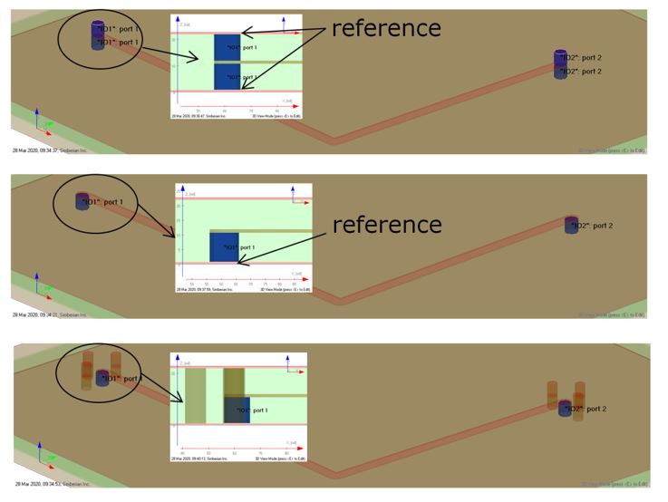
The first case from Figure 1 with ideally equipotential planes is just a model – 2 ports from the trace to the planes are used to excite only a TEM wave. Port construction is illustrated in the top picture in Figure 4.

Figure 4. Trace with ports to two planes (top), with ports to a bottom plane (middle) and with a port to bottom plane with short-circuiting vias around each port (bottom).
Such port construction removes the interaction between the TEM and PPW completely. The excitation port up has a – 1 V source, and the port down is +1 V. That produces no voltage between the planes. On the other hand, the port from the trace to just the bottom plane with +1 V excitation (as shown in the middle picture of Figure 4) produces waves in both transmission line and transmission plane.
We can avoid or reduce such transformations in real life by short-circuiting or stitching vias, connecting the reference planes and enforcing the equipotentiality as shown at the bottom picture on Figure 4. The vias make planes equipotential locally, and the signal goes mostly into the TEM mode of the trace as illustrated in Figure 5 (click on graphic to see animation).
Figure 5. Power flow density in a trace with enforced equipotentiality. The trace segment is excited with a 1 V 50 Ohm, 20 GHz harmonic source at the bottom left port. Another port is terminated with 50 Ohm. Both ports are via-ports with signal terminal at the trace and reference terminals at the bottom plane only. Planes are connected with 3 vias around each port, to enforce the equipotentiality.
The most critical location for such enforcement is the location of the signal via. If a few stitching vias are placed electrically close (within quarter of wavelength in dielectric at Nyquist frequency) to each signal via, the PPW waves will be substantially reduced, and the signal will be transformed into the TEM wave again (see Figure 5). Such equipotentiality enforcement is not possible if two reference planes of the trace cannot be connected or stitched.
The key takeaway here is this: Stackup must be re-designed to allow plane-to-plane stitching around the launch vias and, possibly, along the traces. Otherwise the localization of the transition is compromised with unpredictable consequences [1], [2].
Note: Power flow density is used to illustrate the concept of signal transformation. Planes are assumed infinite that is simulated with perfectly matched layer (PML) boundary conditions.
1. Y. Shlepnev, Life beyond 10 Gbps: Localize or Fail!, Signal Integrity Journal, April 18, 2018.
2. “How Interconnects Work” demo-videos on launch and via localization at https://www.simberian.com/ScreenCasts.php or at Simbeor channel on YouTube https://www.youtube.com/user/simbeor/videos


