Uniform transmission lines are best suited for high-speed data transmission because of their broadband impedance characteristics. In some applications, a minor deviation from uniformity can help in optimizing other desired signal integrity metrics. Channel operating margin (COM) of serializer/de-serializer (SERDES) links is affected by several parameters [1]. Of these, skew (which affects insertion loss) and crosstalk are important contributors. Skew in a printed differential pair due to “fiber weave effect” is well known and many solutions for characterization and reduction exist [2-3]. Methods for the minimization of crosstalk in PCBs have also been well researched [4]. As a possible solution to these two problems, this paper investigates using a non-uniform interconnect geometry.
Interconnect Geometry
A broadside coupled differential pair geometry is known to require thicker dielectric substrates. The edge-coupled differential pair has a primary advantage that it can be implemented with a reduced PCB thickness and layer count as shown in Figure 1. The broadside coupled trace geometry can be modified by offsetting the two traces as shown. This reduces the coupling between traces and the layer thickness required for a given impedance.
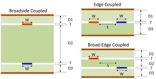
Figure 1: Differential transmission line geometries drawn to scale

Table 1: Dimensions of differential transmission line geometries of Figure 1 in mils (Zs is the self impedance of each trace; Zm is the mutual impedance between traces)
Fiber Weave Skew In PCBs
In PCBs, uniform edge-coupled differential traces are widely used. It can be difficult or even impossible to maintain strict uniformity in a real PCB. Routing in ball grid array (BGA) and connector pin fields is needed, and these present a non-uniform environment. Further, the PCB substrate itself presents a non-uniform environment where fiber glass is used.
Interestingly, these non-uniformities tend to be periodic. By introducing an intentional periodic non-uniformity in the traces of a uniform interconnect, it is possible to correct for the undesirable effects arising from the environment. This has been used earlier to reduce impedance variations and cross talk. By a suitable modification, it can be designed to ensure that each P or N trace of a differential pair perceives the same environment [5]. While there is no apparent advantage in the broad-edge-coupled interconnect, it helps in the construction of a pseudo- twisted pair as shown in Figure 2.
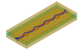
Figure 2: Illustration of a non-uniform differential interconnect.
First consider the case of a straight broad-edge-coupled differential pair as shown in Figure 3. The substrate has three single-ply 1080 style weaves stacked with their weave patterns perfectly aligned to result in a maximum lateral variation in the dielectric constant. The geometry has W = 4 mils, S = 10 mils, D1=D3 = 4 mils, D2 = 3 mils, and T = 0.6 mil. A dielectric constant value of 6 and loss tangent = 0.02 is assumed for the glass bundles. A dielectric constant value of 2 and loss tangent = 0.01 is assumed for the resin. The length of the transmission line is assumed to be 200 mils. (3D EM simulations were carried out using Ansys’ HFSS.)
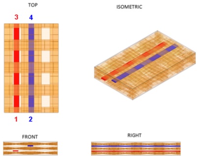
Figure 3: Illustration of a part of a straight 200 mils long broad-edge interconnect geometry used as a reference
Computed s-parameters are shown in Figure 4. Differential pair Diff1 is formed by single-ended ports 1 and 2, and differential pair Diff2 is formed by single-ended ports 3 and 4.
Skew in time domain is obtained from the phase difference of the single-ended insertion loss. From Figure 4, note that at 25 GHz, the phase difference between S13 and S24 is 32.53 degrees. From reference [5], the phase difference in radians is equal to 2 x p x frequency x skew in time domain. This gives a skew value of 3.6ps (32.53/(360 x 25e+09)) for a 200 mil line length. For a trace length of 1 inch it is 18 pS/inch. It can also be seen that this differential pair has very low far-end cross talk (FEXT) between its P and N traces.

Figure 4: Computed s-parameters of the geometry in Figure 3 (Note : S14 < -54 dB)
The non-uniform interconnect, shown in Figure 5, is constructed by sweeping a rectangle (trace cross-section) along a curve defined by the equation


Figure 5: Illustration of a portion of the non-uniform trace geometry.
The N-Trace on a different layer is a mirror image of the P-trace as shown in Figure 5. All other physical parameters are the same as the geometry of Figure 3. Computed skew in this case is less than 0.03pS/inch (see Figure 6).

Figure 6: Computed s-parameters of the geometry in Figure 5
It is easy to see that by controlling the periodicity of the line, the number of overlapping twists can be made to vary. Increasing the number of “twists per unit length” will decrease the P-N skew.
This type of non-uniform transmission line has another unique characteristic as shown in the single-ended coupling plot of Figure 6. Single-ended FEXT (SE FEXT) = S(4,1)) between P and N traces increases with frequency while the single-ended insertion loss (SE IL = S(2,1)) decreases. A short section of this geometry can be used to build a strongly coupled differential pair.
It is important to note that “skew” itself is not a fundamental parameter influencing the COM [1]. Differential insertion loss is strongly affected by skew, which can result in a null at a precise frequency and its integral multiples leading to complete fading. When this frequency approaches the Nyquist frequency of data transmission, eye opening reduces, leading to an increased bit error rate (BER).
If this undesirable effect of skew can be reduced, it will become possible to operate at high data rates even in the presence of substantial skew. It is possible to reduce the effect of skew by the use of strongly coupled differential elements. Two or more of these elements need to be inserted at certain locations along the link path. They result in a significantly reduced fading. This has been validated analytically as well as numerically in reference [5].
Differential Near-End Crosstalk In Packages
In the case of semiconductor packages, high density is commonly achieved using flip chip (FC) and BGA technology. Long-reach electrical interfaces operating at very high data rates need to be designed to meet stringent requirements on the insertion loss, return loss, and crosstalk.
State-of-the-art active devices can overcome large values of insertion loss in the link. However, it is the crosstalk level that limits the maximum length of the link. Near end cross talk (NEXT) is determined by the electromagnetic coupling that occurs in a very small region near the FC bumps. Interconnect differential cross talk levels are generally reduced by increasing spacing between diff pairs and using grounded guard traces. Where the differential pair density is high, closely spaced, and necked, interconnect routing over extremely short distances near the FC balls becomes inevitable and this leads to increased NEXT [6]. By the use of non-uniform traces over a small region, a substantial reduction of NEXT becomes possible [7].

Figure 7: Cross sectional view of differential transmission line geometries. (Dimensions in microns, substrate ABF GZ41, Zs is the self impedance of each trace and Zm is the mutual impedance between traces)
First, to obtain a reference, a 2000 microns long edge-coupled stripline of Figure 7 is simulated. This interconnect is 23 microns wide with an edge-to-edge spacing of 29 microns. Therefore, the end-to-end distance along the cross section is 23+29+23 = 75 microns.
The P-trace of the non-uniform diff pair is constructed by sweeping the rectangular trace cross section (W x T) along a path defined by

The N-Trace is obtained by multiplying y(t) with -1. It is important to note that using a trace width of 25 microns with a spacing of 25 microns will give a differential impedance of 104 Ohms only for straight broad-edge-coupled traces. Constructing a non-uniform trace with the same trace width and space will result in a lower characteristic impedance. Due to the overlapping regions, this geometry has more capacitance and its characteristic impedance is less than that of the uniform line of Figure 7.
This is compensated by reducing the trace width to 18 microns and increasing the gap to 39 microns. For a fair comparison, the end-to-end distance of both cases is fixed at 75um. Therefore, the non-uniform trace is 18+39+18 = 75 microns along its width and 2000 microns along its length.

Figure 8: Computed s-parameters of a single differential pair
Computed results are shown in Figure 8. The non-uniform interconnect will have an increased insertion loss arising from the longer path length and the narrower trace.
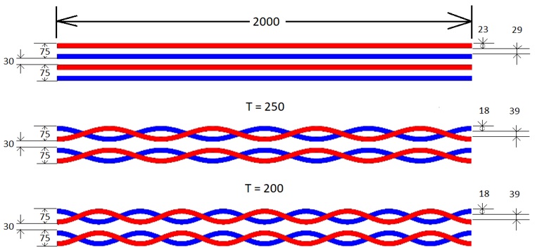
Figure 9: Illustration of the top view of the 3 cases considered (dimensions in microns).
To compare differential crosstalk levels, a pair of traces placed side by side with a spacing of 30um as shown in Figure 9 is simulated. The straight stripline case has the same cross section as in Figure 7.
In 1881, Alexander Graham Bell invented the twisted pair cables to reduce crosstalk. From a radiation standpoint, twists lead to a reduction in the near-field strength and hence cross talk. In the case of twisted pair cables used to carry Ethernet data, it is known that their performance depends on the number of twists per unit length. The non-uniform interconnect geometry in Figure 2 behaves like a twisted pair in two dimensions. Two different twist periodicities are considered for illustration. In the simulations, the end-to-end distance in the cross section is maintained at 180 microns in all 3 cases. That is, each pair is 75 microns wide and are spaced 30 microns apart. All three examples are 2000 microns along the length.
Computed s-parameters show differential insertion and return loss values very close to that in Figure 8 and are not repeated here. Figure 9 shows a comparison of the differential NEXT values, and a reduction of 9dB is feasible with value of T = 250 um which amounts to 8 twists over the length. Increasing the number of twists to 10 along the length only results in a small improvement in the NEXT level.

Figure 10: Computed Differential NEXT comparison for the geometry in Figure 9
It also important to see the effect on FEXT (Figure 10). While FEXT shows some reduction at low frequencies for T = 250 um, it remains nearly the same as the stripline at high frequencies. Increasing the number of twists leads to an improvement in the NEXT level. However, it can increase the FEXT level substantially.
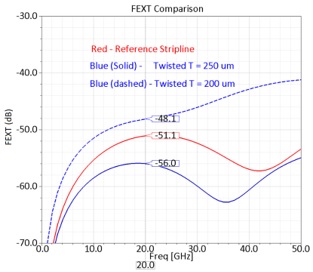
Figure 11: Computed Differential FEXT comparison for the geometry in Figure 9
Conclusion
In this work, a new transmission line structure is proposed as a solution to address fiber weave skew in PCBs and NEXT in packages. In the case of PCBs, it will allow usage of lower cost laminates that are known to cause fiber weave skew. An example is long flex PCBs. In the case of packages, short sections of non-uniform interconnect can be used near the FC region. A disadvantage is the need for an additional routing layer and for a high precision in layer-to-layer registration.
References
[1] B. Gore, and R. Mellitz, “An exercise in applying Channel operating margin for 10GBASE-KR Channel Design,” Proceedings of the IEEE EMC Symposium, Rayleigh, NC., 2014, pp. 648-653.
[2] J. Loyer, R. Kunze, and Xiaoning Ye, “Fiber Weave Effect: Practical Impact Analysis and Mitigation Strategies”, Proceedings of DesignCon 2007, pp. 1-28.
[3] Eric Bogatin, Bill Hargin, Venkata Satya Sai, Don and Don de Groot, “New characterization techniques for glass weave skew” Signal Integrity Journal, March 2017.
[4] Howard Johnson and Martin Graham, High Speed Signal Propagation – Advanced Black Magic, Signal and Power Integrity Simplified, Prentice Hall, 2003.
[5] Syed Bokhari, “On the minimization of PCB Differential pair skew or its effect”, Proceedings of DesignCON 2019.
[6] Pavel Roy Paladhi, Jose Hejase, Nam Pham, Ghadir Gholami, Prasanna Jayaraman, Megan Nguyen, Glen Wiedemeier, and Daniel Dreps Pavel Roy G. Eason, B. Noble, and I. N. Sneddon, “Effect of NEXT coupling in close proximity to Receiver at 25 Gb/s Bus,” Proceedings IEEE 26th Conference on Electrical Performance of Electronic Packaging and Systems (EPEPS), October 15-18, 2017.
[7] Syed Bokhari, “NEXT Reduction in Package Interconnects”, 2019 IEEE 28th Conference in Electrical Performance of Electronic Packaging and Systems(EPEPS), Montreal, Canada.

