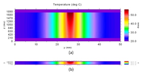
Figure 1(a), taken from our recent book [1], shows a simulation of the vertical heat flow from a trace through a board to the other side. The simulation is for a 100 mil wide, 1.0 oz. thick trace heated to almost 58 oC on the top layer of a 63 mil thick FR4 board. The figure looks impressive, but it is misleading in one very important sense. The horizontal and vertical scales are very different. That image represents a cross-sectional area that is only 63 mils (1.6 mm) thick but 2.0 inches (50 mm) wide.
 Figure 1. Vertical heat flow through a PCB.
Figure 1(b) is the same thermal image shown approximately to scale. What becomes apparent when viewed this way is that there is very little opportunity for horizontal heat flow away from the trace because the board is both geometrically and thermally thin. That means that the bottom layer of the board will have (approximately) the same thermal profile as the top layer. That means that all layers in between will also have that same thermal profile – current through a trace heats not only the trace, but also everything underneath it.
Heated Pads
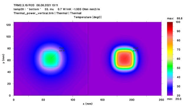
Recently, we ran an interesting set of simulations (see [2] and [3]) exploring this relationship further. Figure 2 represents part of that simulation. We start with a 250 x 125 mm FR4 board, 1.6 mm thick. Two copper pads, 25 x 25 mm, are placed on the top layer. The copper pads are heated by applying 2.5 Watts of power to them. A copper plane, 125 x 125 mm, is placed on the bottom layer on the left side of the board only.

Figure 2. Two pads heated with 2.5 watts. Left pad has a large plane under it.
The applied power heats the pad on the right (no underlying plane) to 93 oC, 73 oC above the ambient. Placing a plane underneath the pad (left side of image), lowers the pad temperature to 59 oC. But what is truly interesting is what happens on the bottom layer, shown in Figure 3.
 Figure 3. Bottom Layer of the board shown in Figure 2.
The thermal profile of the bottom layer (Figure 3) looks very similar to that of the top layer (Figure 2). The temperatures are nearly the same, also. The top layer temperature of the heated pad on the right is 93 oC. The same area on the bottom layer is approximately 89 oC, only 4 degrees cooler than the top layer. The temperature of the area underneath the left pad is approximately 50 oC, 9 degrees lower than the top pad.
So, what if we put the plane on an internal layer of the board? Figure 4 illustrates the thermal profile of the bottom layer when a plane is placed on an internal layer 0.5 mm below the left-hand pad. The right-hand area under the heated pad is still only 4 degrees cooler than the pad on the top layer. The closer plane lowers the temperature of the left-hand pad on the top layer to about 45 oC. The corresponding temperature on the bottom layer is about 39 oC, 6 degrees cooler than the top layer temperature.
 Figure 4. Thermal profile of bottom layer if an internal plane is placed 0.5 mm below the top layer.
It is interesting to note that the presence of a copper plane tends to lower overall temperatures, because of better horizontal thermal heat flow, but it has much less effect on the overall thermal pattern. Even with a copper plane on the bottom layer (Figure 2), the thermal profile on the plane resembles the thermal profile above it. There can be (and are) significant thermal gradients on copper surfaces and planes, a point emphasized in numerous places in our book [1].
These results illustrate an important truth: the thermal profile of the bottom layer of a circuit board resembles the thermal profile of the top layer. The difference in spot temperatures is typically less than 10 oC between the top and bottom layers and is more often in the range of 5 oC or even less.
Heated Traces
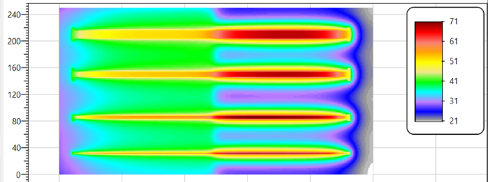
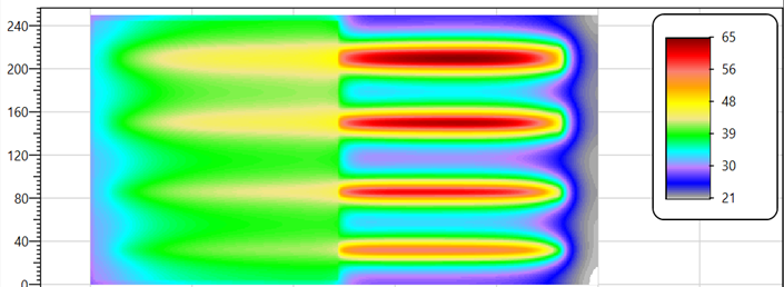
Now these pads are relatively large. What if we look at normal sized (heated) traces? We replaced the pads in the simulations with four traces, 1, 2, 4, and 6 mm wide (approximately 40, 80, 160, and 240 mils, respectively). Each trace carries enough current to raise its temperature (without an underlying plane) to about 70 oC. A simulated plane was placed on the bottom layer for the left-hand half of the board. Figure 5 shows the thermal distributions of the top and bottom layers of the simulation.
Top Layer
 Bottom Layer
Figure 5. Thermal profiles of top and bottom layers simulating heated traces. In this simulation there is a plane on the bottom layer, left side of board.
We also simulated this board with a plane 0.5 mm below the traces under the left-hand side of the board (not shown). The results are tabulated in Table 1. The important results are in the Difference “Diff” columns for each planar configuration (none, bottom layer, internal layer).
 Table 1. Results of Trace-Level Simulations (Temperature in oC).

