As with any design decision, selecting a backplane design approach requires tradeoffs in price, flexibility, and performance specific to a particular network topology. This article analyzes the effect on high-speed serial-link performance for a printed circuit board (PCB) backplane versus a backplane constructed of connectorized cable assemblies, particularly in terms of IEEE and OIF compliance specifications, and notes what kinds of applications might be well suited for a cable or PCB backplane.
Should I use a cable or PCB backplane in my system design? As with most questions regarding signal integrity, the answer is: it depends. In this article, we take a close look at signal integrity implications at the component and system levels for applications that require a backplane, noting performance opportunities as well as integration tradeoffs and advantages.
At the BOM level, a cable backplane can be more expensive than a traditional PCB backplane. But, at the system level, it can offer significant advantages by enabling earlier software development and integration activities in the front end and lower total cost of ownership on the back end. For instance, a cabled backplane can offer the flexibility to interface blades with test equipment, software development platforms, and early engineering prototype systems, all while offering high enough performance to futureproof the production solution. Additionally, the improved channel performance, or reach, with cable assemblies as compared to PCB routes can be used in some case to increase network spans and physically reach more nodes.
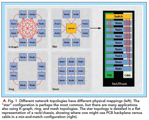
Figure 1 shows physical mappings for several common network topologies. In the case of the star topology outlined in the rack/chassis in the right side of the figure, the node or blade can be the same design with the same connectors, regardless of whether it has a cable or PCB backplane. As a result, it is possible to design for a PCB backplane today and migrate to a higher-speed cable backplane later, or design for a cable backplane today to achieve extra margin. This would allow for insertion of new blades and switches in the chassis later, netting substantial design and system reuse. When used as an Agile systems integration on/off ramp and potential product life cycle extender, the upside opportunities offered with cabled backplane approaches can vastly outweigh differences in component cost.

Backplane Performance


Figure 3 shows the modeled and simulated insertion loss between the topologies, described in Figure 2, with two different length options for each type of topology. The significant change is the loss between the pink traces (PCB backplane 2 and 16 in.), with the most loss in the 16 in. PCB backplane channel still providing approximately 6 dB of insertion loss margin. But is that enough? Answering this requires performing system level channel analysis.

System Level Channel Analysis

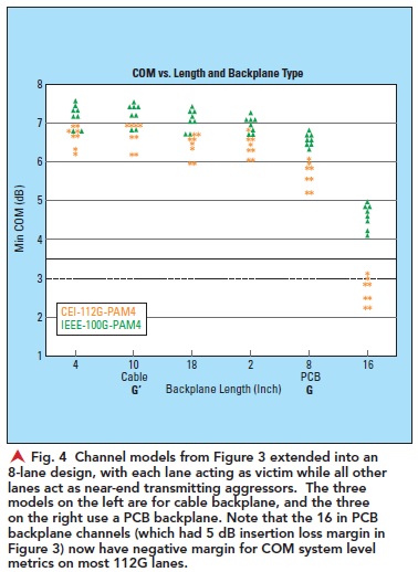
In this model of 800 GbE ports, each lane acts as a victim while the seven other lanes act as near-end transmitting aggressors. In Figure 4, the green points are at CEI-112G-LR-PAM4 while the orange are at IEEE 802.3 400GBASE-KR4; the three plots on the left are for cable backplane (G’) while the three on the right are PCB backplanes (G).
In the past, the 6 dB margin demonstrated in Figure 3 would be a comfortable place for the designer to stop development and analysis, confident that unaccounted for error terms would be small in comparison. For 112G and higher, that is no longer the case and channels must be assessed with true end-to-end multi-lane effects at the system level including all significant regions of interconnect. Connector systems that offer options for both board-to-board and cable-to-board interconnects can be used to navigate the design trade space and offer significant opportunities for earlier integration and longer sustainment.

