The need for high bandwidth links continue to grow to meet the demand of high performance computing, data centers, servers and storages driven by internet in general and multi-core memory and processors architectures in particular [1]. The high bandwidth necessitates a large increase in the interface data rate and width.
In the past, the growth of data rate has been sustained by increasing the performance of the input/output (I/O) circuits and the use of more complex equalization, complicated coding and modulation and other signal processing techniques. Subsequently, the electronic and I/O power consumption significantly increases with increasing the interface speed. Thus, the link data rate increase cannot only come from circuit design and performance improvements.
The passive channel, printed circuit board (PCB) on which the electronic components are based on, impose limitation on the supported speed. In today’s backplane, the maximum capability of the copper backplane determines the performance of the system. Starting with high-end systems, the transfer from copper backplane to an optoelectronic backplane has been anticipated for a while. Even though, the gap between optical and electrical interconnects are reducing in terms of component cost, and manufacturability, electrical interconnect have still been cost and power efficient solutions for backplane links at present time. To improve and extend the reach of copper-based interconnects, several improvement have been suggested to high-speed channel using low-loss dielectric, smooth copper surfaces, improved connectors and packages [2]-[3].
The viability of copper-based interconnect systems utilizing advanced connectors, packages, and boards with low-loss laminates are not anymore in doubt for data rate of 25 Gbps [4]. In order to enable higher data rate links, for 100 Gb/s Ethernet routers and switches and other high-end systems, backplane serial links with data rates beyond 25 Gbps are being standardized using copper-based interconnects and low-loss boards [5]. There are proposals for the next generation standards of electrical signaling to run at several data rates beyond 50 Gbps across low-loss board over 0.5 m long and cables over 1 m long.
The design of interconnects that support data rates exceeding 50 Gbps is necessary to support Terabit backplane systems. In order to predict and optimize the performance of high-speed links operating at 50 Gbps and beyond, it is essential to accurately model and characterize the interconnect systems. The models of interconnects have to be broadband and include high frequency effects that were not critical at that data rates in the range of 10 to 20 Gbps [6]. For higher data rates, very careful modeling of signal propagation in PCB and package traces requires proper identification of the conductor and dielectric frequency-dependent properties over an extremely wide frequency band. In addition, 3D modeling and characterization of transition structures is essential to understand and optimize the wave propagation and minimize mismatch across various transition structures, such as via and BGA at the interface between package and PCB.
Low-loss laminates, such Megtron 6 from Panasonic, FR408HR from Isola Group, and Nelco 4000-13 EPSI from Park Electrochemical Corp., are expected to be key enablers to design boards to run at higher data rates. These laminates offer much more stable dielectric characteristics and have considerably less loss at high frequencies. To investigate the effect of low-loss laminates and see the impact of surface roughness, dielectric properties, glass weave effects, we compared several boards with Megtron 6 with Hyper Very Low Profile (HVLP) finish and Reverse-Treated Foil (RTF) finish, Nelco 4000-13 EPSI with RTF copper foil and standard glass weave, Isola FR408HR with RTF copper foil and standard glass weave. Table I shows typical electric properties of these low-pass laminates that are studied in this paper and of a typical FR-4 board for comparison. Figure 1 shows the photo of some of the boards designed to characterize the traces and the dielectrics.
Table I: Electrical properties (dielectric constant, loss tangent or dissipation factor, and amplitude of surface roughness of laminates studied.


Figure 1: Some of the boards designed for material characterization showing locations of probe pads and MMPX connectors.
Several structures, including microstrips and striplines of various lengths with probe pads and connectors, were designed. Additional structures were also included on the board to improve and minimize de-embedding procedures. The pad-to-pad links of two set of differential nets of 6-in. and 12-in. long striplines, shown in Figure 2, were used to characterize the low-loss materials and traces.

Figure 2: The cross-section of the 8-layer board with 6 in. and 12 in. striplines designed on the 4th layer and the launch structures.
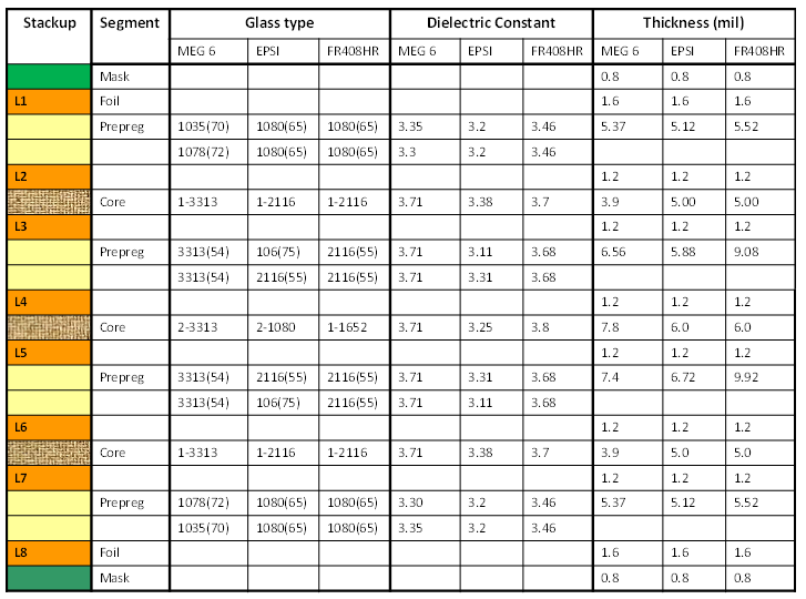
The stackup of the boards, the glass type, the material family, the dielectric constant at 1 GHz, and the thickness of the layers are summarized in Table II. The material properties and dimensions are provided by the manufacturer as typical values and need to be verified for the specific boards manufactured for these experiments.
Table II: Layer stackup, glass types, dielectric constant at 1 GHz, and thickness for Megtron 6, Nelco N4000-13EPSI, and FR408HR boards.
First, the manufactured boards were cross-sectioned to accurately verify all the dimensions of the transmission lines. Figure 3 shows the cross-section of the board with Isola’s FR408HR, Nelco N4000-13 EPSI, Megtron 6 with RTF and HVLP finishes. The dimensions for the conductor thickness, width, the trace spacing, and the top and bottom layer heights are all marked in microns 
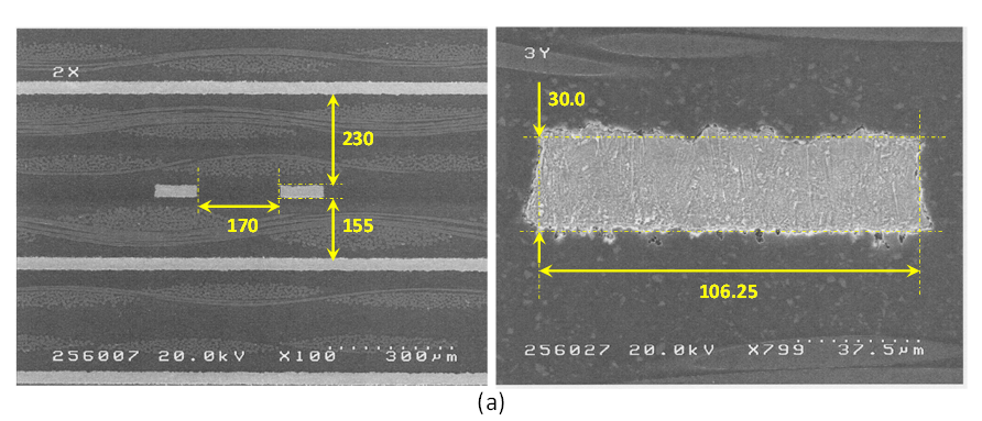
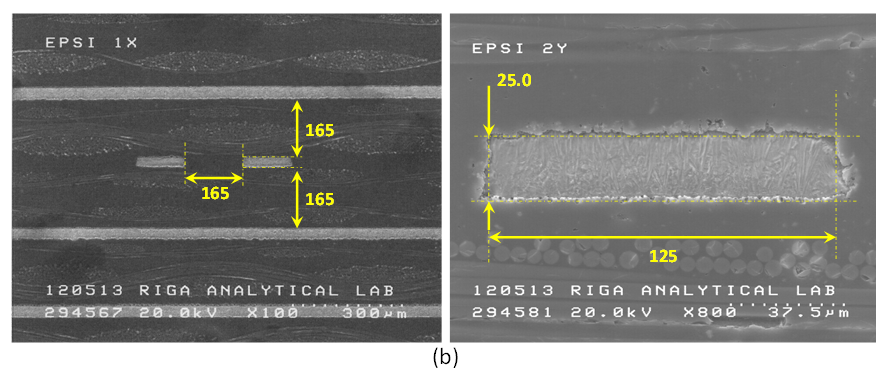

 Figure 3: Micro-photographs of cross-sections of the traces showing copper roughness, (a) FR408H, (b) Nelco N4000-13EPSI, (c) Megtron 6 RTF, (d) Megtron 6 HVLP boards
Scattering parameter measurements were taken with a 4-port 67-GHz vector network analyzer (VNA) using high-frequency probes with 200 um-pitch GSSG configuration and high-frequency snap-on connectors. The two set of differential nets with 6-in. and 12-in. long traces for FR408HR, Nelco N4000-13 EPSI, Megtron 6 with RTF, and HVLP finish were measured. The measured differential and common mode insertion loss for the 12 in. traces of the four boards is show in Figure 4. The simulated insertion losses of similar structures using FR4 boards are also plotted for comparison. The plots show attenuations that agree with the electrical properties of these laminates given in Table I. The measured differential insertion loss of the Megtron 6 with HVLP finish shows about 2 dB improvement over that of the Megtron 6 with RTF finish at 25 GHz. The Megtron 6 with HVLP finish also shows about 4 dB and 6 dB improvements over Nelco N4000-13 EPSI and FR408HR, respectively. The 12-in. trace in Megtron 6 with HVLP laminate shows about 20 dB less loss when compared to similar trace in FR-4 board.
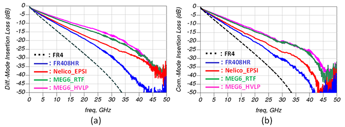
Figure 4: Magnitude of the measured (a) differential and (b) common-mode insertion losses are shown for the four boards: Megtron 6 HVLP (pink), Megtron 6 RTF (Green), Nelco N4000-13 EPSI (red), and FR408HR (blue). The insertion loss of typical FR-4 board is also shown from simulation (black dashed line).
The differential group delays of the 12-in. traces are calculated from the measured four-port S-parameters. The delays per inch of the four boards are plotted as functions of frequency in Figure 5 (a). The simulated group delay for FR-4 board is also included in the plots. The Nelco N4000-13 EPSI shows the smallest delay as expected from the dielectric constant value of this laminate given in Table I. The typical FR-4 shows the longest delay as predicted from its higher dielectric constant.
Time-domain simulations are also performed using the measured S-parameters to calculate the single-bit response for an excitation of a pulse with amplitude of 1 V and width of 20 ps (corresponding to a data rate of 50 Gbps) and rise and fall time of 8 ps. Figure 5(b) shows that the single-bit responses of the Megtron 6 board experienced the least attenuations as predicted by glancing at the differential insertion loss shown in Figure 4(a). On the other hand, the single-bit responses for FR-4 suffered the larger attenuation and edge degradation closely followed by FR408HR when compared to the Megtron 6 boards. Although the single-bit response of the Nelco N4000-13 EPSI suffered similar attenuation and dispersion as FR408HR, it experienced the least delay due to its low dielectric constant.
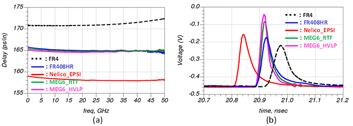
Figure 5: (a) The delays per inch and (b) the single-bit responses (at 50 Gbps) of the 12-in. long traces are shown for the four boards: Megtron 6 HVLP (pink), Megtron 6 RTF (Green), Nelco N4000-13 EPSI (red), and FR408HR (blue) and FR-4 (black). The group delay and pulse response of FR4 board are from simulation.
Next, we used the measured S-parameters measured of the two stripline of length of 6 in. and 12 in. to identify broadband dielectric and conductor roughness models using the generalized modal S-parameters [7]-[8]. The detail of the method is explained in the next section. The ability to properly separate conductor and dielectric losses for a wide range of cross-sections and low-loss dielectrics is very critical to construct models that agree with measured data for wide-range cross-section used in board design. The accurate transmission line and transition models are then used for performing analysis and optimization of high-speed interconnects operating at 50 Gbps.
To read the rest of this paper, Download the PDF. This paper was originally presented at DesignCon 2014.
References
- A. F. Benner, et al., “A roadmap to 100G Ethernet at the enterprise data center,” IEEE. Communications Magazine, vol. 45, no. 11, pp. 10-17, Nov. 2007.
- R. Kollipara, et al., “Practical design considerations for 10 to 25 Gbps copper backplane serial links,” in IEC DesignCon, Santa Clara, CA, Feb. 6-9, 2006.
- H. Braunisch, et al., “High-speed flex-circuit chip-to-chip interconnects,” IEEE Transactions on Advanced Packaging Technologies, vol. 31, no.1, pp. 82-90, Feb. 2008.
- D. G. Kam, et al., “Is 25 Gb/s on-board signaling viable?,” IEEE Transactions on Advanced Packaging Technologies, vol. 32, no.2, pp. 328-344, May 2009.
- IEEE P802.3bjTM 100 Gb/s Backplane and Copper Cable Task Force, http://www.ieee802.org/3/bj.
- W. T. Beyene, et al., “Advanced modeling and accurate characterization of a 16 Gb/s memory interface,” IEEE Transactions on Advanced Packaging Technologies, vol. 32, no.2, pp. 306-327, May 2009.
- Y. Shlepnev, Modeling frequency-dependent conductor losses and dispersion in serial data channel interconnects, Simberian App. Note #2007_02, http://www.simberian.com/AppNotes.php
- Y. Shlepnev, Modeling frequency-dependent dielectric loss and dispersion for multi-gigabit data channels (with experimental validation), Simberian App. Note #2008_06, http://www.simberian.com/AppNotes.php
Author(s) Biography
Wendemagegnehu (Wendem) T. Beyene received his B.S. and M.S. degrees in Electrical Engineering from Columbia University, in 1988 and 1991 respectively, and his Ph.D. degree in Electrical and Computer Engineering from University of Illinois at Urbana-Champaign, in 1997. In the past, he was employed by IBM, Hewlett-Packard, and Agilent Technologies. He is currently a technical director at Rambus Inc. where he is responsible for signal and power integrity of multi-gigabit serial and parallel interfaces.
Yeon-Chang Hahm received his M.S. and Ph.D. degrees in Electrical and Computer Engineering from Oregon State University in 1997 and 2000 respectively. His academic research area focuses on computing distributed elements of on-chip interconnects and modeling. After receiving his degree, he joined IBM, AMD consecutively and worked on SI/PI area for 12 years. He is currently a Principal Engineer at Rambus Inc. responsible for electrical modeling of on-board & on-package passives as well as SI simulations of high-speed serial and parallel signals.
Jihong Ren received her PhD degree in Computer Science from University of British Columbia, Vancouver, Canada in 2006, where she worked on optimal equalization for chip-to-chip high-speed buses. She is currently a Senior Manager at Altera, managing the SerDes IO architecture group. Prior to Altera, she was with Rambus Inc., managing the Signal Integrity and Power Integrity team. She authored and co-authored more than thirty papers, four book chapters and filed 14 patent applications in high-speed communications area. She was awarded the silver Distinguished Inventor award from Rambus in 2010.
Dave Secker is currently a Technical Director in Systems Engineering at Rambus Inc., where he has been for the past 17 years. His responsibilities include physical design, modeling and optimization of high-speed signal interconnect and power delivery networks at the IC package and system board levels. Previously he worked at Los Alamos National Laboratory as a research assistant. Mr. Secker received his M.S. degree in Electrical and Computer Engineering from The University of Arizona in 1996.
Don Mullen is currently a Senior Principal Engineer at Rambus Inc., focusing on systems packaging, mechanical, and thermal design; he has been at Rambus for the past 15 years. Prior to Rambus, he held various engineering positions involving electronic packaging, thermal design, biomedical engineering, and mechanical systems engineering design. He has a BSME (’70) and is a registered professional engineer in California..
Dr. Yuriy Shlepnev is President and Founder of Simberian Inc., where he develops Simbeor electromagnetic signal integrity software. He received M.S. degree in radio engineering from Novosibirsk State Technical University in 1983, and the Ph.D. degree in computational electromagnetics from Siberian State University of Telecommunications and Informatics in 1990. He was principal developer of electromagnetic simulator for Eagleware Corporation and leading developer of electromagnetic software for simulation of signal and power distribution networks at Mentor Graphics. The results of his research are published in multiple papers and conference proceedings.

