
An expert is someone who has made all the mistakes possible. However, one does not have to have made all the mistakes firsthand, as long as one can learn from the mistakes of others.
A board recently built by a student showed a strange resonance, which took a bit of sleuthing to resolve. Figure 1 provides an example of the return and insertion loss (IL) of a simple uniform transmission line, showing the sharp suck-out at about 9.4 GHz.
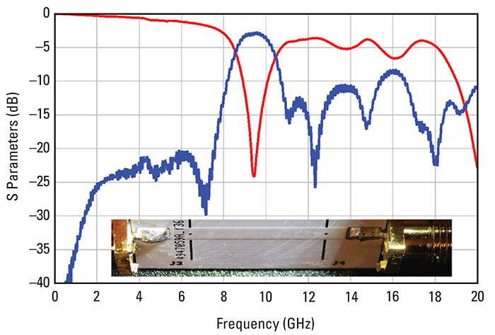 Figure 1. Measured insertion and return loss of a uniform transmission line, shown in the inset. Where is the resonance coming from?
This sort of sharp dip in IL and a corresponding peak in the return loss (RL) is a signature of a resonance. But where was the resonance coming from? It was just a simple, short transmission line.
Now that the root cause of this anomaly is understood, it can be avoided. Here is the lesson that was learned.
What to Avoid During Design
This simple board was a 2-layer board, with a solid ground plane on the bottom layer. The SMA ground pins were soldered to the bottom of the ground plane and the signal pin was soldered to the top signal trace. This sort of suck-out in the IL is an indication of a resonance stub somewhere. But there were no vias on this board, and there were no routing stubs anywhere. What was resonating? It turned out to be a thermal relief feature in the ground pad of the SMA connector.
The purpose of the thermal relief is to aid in the assembly of the circuit board. A thermal relief structure creates a short isolation “moat” or a gap in the solid copper, with a few very short “bridges” that span the gap to provide an electrical connection. The moat provides thermal isolation, and the bridges provide electrical connection.
While a solid copper flood connection gives the best electrical performance, it also serves as a heat sink for pins connected to a plane. This sink will effectively pull the heat away from the pin during soldering and may produce poor solder joints in the connection. A thermal relief structure for ground vias is important when soldering through-hole pins connecting to the ground plane.
When adding the pad to solder the SMA ground leads, the EDA tool, in its infinite wisdom, automatically adds a thermal relief structure. This structure, shown in Figure 2, inadvertently introduced a signal integrity artifact. This is an example of the law of unintended consequences.
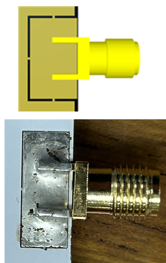 Figure 2. Examples of the thermal reliefs added to pads to make soldering more reliable.
When a signal is launched into the SMA pin from an external source, the return current will cross this slot in the pad and induce a “slot wave mode” of current between the copper edges of the slot.
Once launched into the slot, the signal will propagate down the slot between the edges, to the short, narrow tabs (bridges) that look like an electrical short across the slot. The slot wave mode will rattle back and forth between the shorts, creating a resonance. Since the slot wave cavity has the same boundary conditions on both ends, the resonances arise when a multiple of half wavelengths can fit between the ends of the cavity. The first resonance frequency is roughly: 
The shorter the distance between the shorting tabs, the higher the resonant frequency. When the length is 0.5 in., the resonant frequency is about 6 GHz if the effective Dk is 4. There is an uncertainty related to the unknown Dk_eff when the dielectric is inhomogeneous, such as when the plane is a surface layer.
A Test Board
It is good practice in a lab to approach all problems with a three-tiered approach:
- Analyze the problem based on first principles to identify and understand the root cause
- Simulate the problem to verify that the effect can be turned on and off
- Design, build, and measure a test vehicle to demonstrate the best design practices to eliminate the problem and pathological practices that accentuate this problem.
The test board designed to explore the resonances from slots is divided into two sections. The upper half of the board had thermal relief slots in the return plane in the footprint of the launch. The bottom half of the board had no thermal relief slots at the launches, but had slots of various dimensions introduced beneath the trace. The slot wave mode in the slots was driven by the return currents of propagating signals. Figure 3 shows the board and a few of the slots that were intentionally introduced.
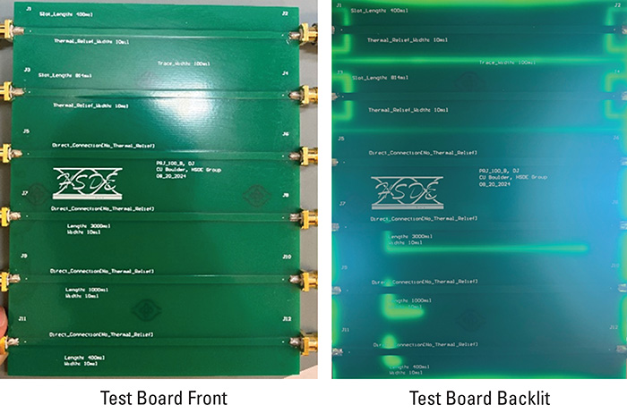 Figure 3. The test board displays the slots under the signal line when backlit.
Measurement Analysis
For an ideal PCB transmission line, the RL (S11) at low frequency should be a large negative dB value, and the IL (S21) should be 0 dB at low frequency. The IL will decrease with frequency due to losses. The presence of a slot to which the return current couples will suck out energy at the slot wave resonant frequency. This will also result in a higher impedance and a larger RL at the resonant frequency. The first example illustrates the ability to turn this slot wave mode off and on.
Two identical 50 Ω test lines were constructed, one with the thermal relief slots in the SMA launch and one without the thermal relief. Figure 4 shows the comparison of the IL of these two lines.
 Figure 4. IL plot for the transmission lines, with and without thermal reliefs.
An important consistency test is to estimate the frequency at which one would expect the slot wave mode resonant frequency. Given its length of 0.4 in., and roughly estimating the effective Dk as 3.0, the expected resonant frequency is 8.51 GHz. This is remarkably close to what is measured, which is 8.6 GHz.
The combination of turning this effect off and on and estimating the magnitude is strong confirmation of the suspected root cause.
Additional Examples
This analysis suggests that any slot in the return plane that return current couples to will drive a slot wave mode and suck out energy in the IL. A few slots in the return plane under the signal line illustrate this. Figure 5 shows a close-up of three of these structures and their measured IL.
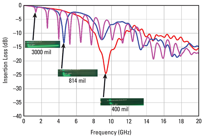 Figure 5. Measured IL and a close-up of the slots introduced under the signal traces.
In these structures, the slot was made 30 mils wide. This increases the contribution from the air and decreases the effective dielectric constant compared to the thermal reliefs.
The measured IL of each slot clearly shows the suck-out at increasing frequency as the length is decreased.
Calculating the resonant frequency for each requires an estimate of the effective Dk. This is a combination of the bulk value and the contribution of the air in the slot wave mode. For this 59 mil-thick board and 30 mil-wide slot, a value of 2.4 gives a prediction of the resonant frequencies for all three slots that matches to better than 5%, as summarized in the Table 1.

Implications
This case study has pointed out one consequence of a signal passing over a slot in the return plane. A slot under one or more signal traces will generate the trifecta of noise. It will induce a slot wave resonance and suck energy out of the signal, and act as a discontinuity to create reflection noise. It will contribute to long-range cross talk to any other signal lines passing over this slot. And the slot wave mode signal will also act as an antenna and radiate.
This unexpected slot in the thermal relief pads was inadvertently added by the EDA tool. However, similar slots are also added to boards with split plane layers that are also used as return planes. This is why the best practice is to use solid return planes adjacent to all signal layers. If split power planes are used, do not use them as return planes.
One can estimate the resonant frequency of the slot wave mode as roughly 3 GHz/Length (in.) using a simple rule of thumb. If the slot is short enough, the resonant frequency can be pushed to a bandwidth well above the signal bandwidth in an application.
However, if it is a long slot, such as found in split power planes, it could create a resonance easily below 1 GHz, where many signal bandwidths lurk. Avoid making this mistake when designing a board.
Conclusion
Designing circuit boards is often like playing the whack-a-mole game. A change is made in one aspect of the design to fix a problem, only to have another problem pop up somewhere else. To reduce the problem of soldering on SMA connectors in an edge launch, a significant signal integrity problem has been introduced.
To reduce the problem of coupling to slot wave resonances, avoid using thermal reliefs in pads where the SMA is launched. However, if opting to use thermal reliefs, make sure the resonant frequency is well above the signal’s bandwidth for the given application. Learn from this inadvertent mistake.
REFERENCES
- E. Bogatin, “What is the Resonant Frequency of a Cavity?: Rule of Thumb #30,” July 2016, Web: https://www.edn.com/what-is-the-resonant-frequency-of-a-cavity-rule-of-thumb-30/
- E. Bogatin, “Sheet Inductance of a Cavity: Rule of Thumb #16,” September 2014, Web: https://www.edn.com/sheet-inductance-of-a-cavity-rule-of-thumb-16/.
- E. Bogatin, “Signal and Power Integrity – Simplified, (Signal Integrity Library),” Third Edition, January 2018.