
The voltage regulator module (VRM) is at the foundation of power integrity, making proper selection essential. There are thousands of VRMs and VRM controllers available from many manufacturers. They are often selected based on size, efficiency, price, or a relationship with the manufacturer. This often leads to a poor VRM selection, requiring additional engineering resources, greater time to market, as well as higher BOM costs to correct the deficiencies.
Even after the VRM or VRM controller is selected, the manufacturer’s guidelines and capacitor selection recommendations can be counterproductive. In this article, we'll evaluate the choices, define some useful figures of merit, and provide specific selection suggestions.
Introduction
Manufacturers are growing more reluctant to share relevant part details needed to ensure an optimum design. Engineers are also overwhelmed with choices, so many engineers choose to follow manufacturer-provided reference designs while accepting the datasheet parameters at face value. The datasheet is typically missing critical information needed to make design trade-offs or develop a reasonable simulation model, including statistical tolerances.
In our analysis work, we frequently find that in addition to the missing data, much of the data provided by the manufacturer is misleading, incorrect, test-equipment or test-setup limited, or just poor quality. The missing or inadequate data means we can’t create an accurate simulation model needed for optimization of the design, worst-case tolerance assessment, or system level design. Some manufacturers provide simulation models, though the fidelity, hardware correlation, and documentation are frequently poor or non-existent. A switching type model is often supplied, which is of very little use in the design process.
Adding to this already uncertain situation, many newer VRMs have “novel” or “unique” schemes to improve transient response. Many of these schemes result in “novel” or “unique” design issues.
The selection of the VRM needs to be based on complete and accurate characterization data comparing several candidates using appropriate figures of merit and occurring BEFORE the circuit board is designed and the decoupling chosen.
Small Signal Considerations
The VRM connects to the system at the input interacting with the input filter and the downstream PDN. It is represented as a 2-port element. The 2-port element results in four performance parameters, identified in Figure 1.

Figure 1 The VRM is represented as a two-port element.
The input impedance presented by the switching VRM is negative, leading to stability concerns related to the source impedance of the bus connected to the converter’s input. The interaction between the switching VRM IC and the input filter, or bus impedance, is well documented and is generally assessed using minor loop gain assessment methods. The loop gain is designated TM_in, and defined as:

The power rail voltage noise (ripple, etc.) is related to the output impedance of the VRM interacting with dynamic variation of the load current (AC portion). A minor loop, designated TM_out, exists on the output side of the VRM and can be represented as:

The stability of both the input and output connections are dependent on the system damping, defined in large part by capacitor ESR on the output side and filter damping networks or capacitor ESR on the input side.
Input source noise (e.g. bus ripple) transfers to the output of the VRM through the power supply rejection ratio (PSRR) while output dynamic current transfers back through to the input filter as an input current perturbation through the VRM’s reverse transfer characteristic.
The performance of the VRM and, therefore, the system, depends on the ability to define and optimize these four key parameters. Optimization is best achieved using simulation, which requires an accurate small-signal state space average simulation model.
A Mathematical Look at Topologies
The most common VRM is the non-isolated synchronous buck topology, shown functionally in Figure 2.
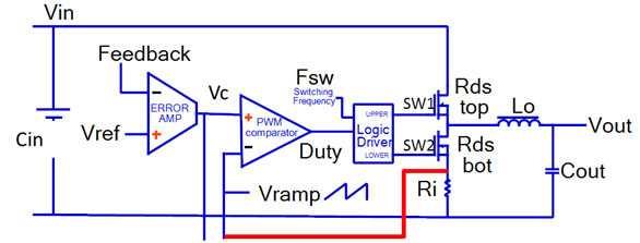
Figure 2 Functional block diagram of the non-isolated synchronous buck topology VRM.
Two common control loop schemes are current mode control and voltage mode control. Both modes compare an error amplifier output signal to a sawtooth ramp. The current mode topology sums an inductor related current signal with the ramp.
A unified model is presented here and discussed in several of the references. It includes user defined current and sawtooth ramp signals, supporting both modes of operation, as well as providing a path to performance optimization.
Each of the four VRM performance parameters can be written in simple form. The low frequency reverse transfer and input impedance are only dependent on the input and output voltages and operating power level.

The PSRR and output impedance (Rout) are much more complex and are dependent on the sawtooth ramp, current sense signal, error amplifier transfer function, output inductor, MOSFET parameters, and the switching frequency.

These relationships show that the characteristics of the sawtooth ramp and the current sense signal must be well defined to construct an accurate simulation model.
Voltage Mode vs. Current Mode Control
The plant gain, defined as the transfer function from the output of the error amplifier, Vc, to the VRM output, Vout, is different for voltage mode and current mode control. The plant gain associated with voltage mode control is shown in Figure 3. It shows a resonance due to the output filter, which results in a second order pole and a gain that varies with input voltage and ramp amplitude. The plant gain associated with current mode control shows a resonance due to the peak current mode sampling at half the switching frequency. The Q is nearly infinite at 50% duty cycle and reduced at lower and higher duty cycles. The Q is damped by the addition of a sawtooth ramp. The plant gain is optimized by the magnitudes of the sawtooth ramp and the current sense signal as seen in Figure 3 and Figure 4.

Figure 3 Plant gain of voltage mode converter for various sawtooth ramp amplitudes.


Figure 4 Plant gain of current mode converter for various sawtooth ramp amplitudes at 25% and 50% duty cycles.

The PSRR performance is shown to be dependent on both the sawtooth ramp and the current sense signal in equation 5. In addition, there is a PSRR null that appears at a specific relationship between these two signals. The null offers the optimum PSRR performance occurring with a ramp signal amplitude defined by equation 9.

An example of this null is seen in Figure 5.

Figure 5 The PSRR null, occurs at a specific ramp signal amplitude and offering optimum PSRR performance.
Current mode control offers much better PSRR than voltage mode while the current mode can be optimized to operate close to the PSRR null. Optimizing PSRR performance minimizes VRM noise while also allowing more of the noise budget to be allocated to other noise sources.
The output resistance is dependent on the current sense signal and the sawtooth ramp and is quite different for voltage mode control and current mode control.

Large values of the sawtooth ramp result in purely voltage mode control, in which case the output resistance is very low and defined by the DCR of the output inductor and the MOSFET switch resistance. These parameters both have large tolerances, making it difficult to maintain a consistent, flat impedance--the foremost goal of PDN design. As the ramp signal is reduced, the open loop resistance increases substantially. These characteristics are seen in Figure 6.

Figure 6 The output resistance of the open loop power stage is significantly different in voltage mode control (lower Vramp levels) and current mode control (lower Vramp levels).
The output impedance sensitivity to the large tolerances associated with the inductor DCR and the MOSFET switch resistance are seen in Figure 7. Current mode control is nearly insensitive to these large tolerances while voltage mode control is highly sensitive.
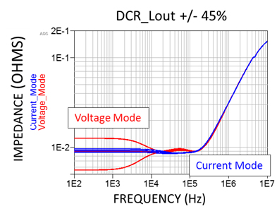
Figure 7 Current mode control is nearly insensitive to the large inductor and MOSFET tolerances while voltage mode is highly sensitive.
The Feedback Amplifier
Many, if not most, newer VRM controllers employ transconductance feedback amplifiers. Transconductance amplifiers offer wide bandwidth and low cost. Manufacturers typically recommend shunt termination of the transconductance amplifier output as shown in Figure 8.

Figure 8 Manufacturer recommended transconductance amplifier shunt termination.
The voltage gain of the amplifier can be calculated as a function of the resistor values and the amplifier transconductance, Gm, while the sensitivity of the amplifier gain with respect to the transconductance can also be calculated.

The large signal amplifier voltage swing is related to the maximum amplifier source and sink current.

Figure 9 Transconductance amplifier with series feedback termination.
While the feedback resistor in the series termination is much larger than the shunt termination it can be set to a value that matches the shunt terminated gain.
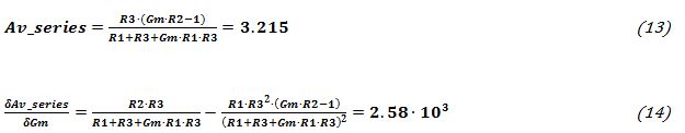
The series termination configuration is a better alternative, offering much lower sensitivity to variations in transconductance evident by comparing equation 12 and equation 14. This sensitivity translates directly to the sensitivity of the closed loop functions – PSRR and output impedance.
Some VRMs include the shunt termination internal to the controller and, in this case, there are limited options for optimization. Without an accessible amplifier output, determination of the amplifier parameters is also difficult.
Summarizing the Small Signal Figures of Merit
The small-signal PSRR and output impedance can easily be optimized using the equations provided here. They can also be used to develop a simulation model. The key variables that must be optimized in the design are the power stage transconductance, 1/Ri, sawtooth ramp, Vramp, and error amplifier transconductance, Gm. The VRM figures of merit that impact design quality are:
- Mode Control: Current mode control outperforms voltage mode control
- Current signal: Ri has an optimum value that is related to the sawtooth signal, Vramp. The sawtooth signal has an optimum value that is related to Ri
- The ratio of sawtooth to ramp signal is key to optimizing the PSRR and the output impedance flatness.
- Gm: The error amplifier Gm is a significant term in the control loop gain Av, as is the gain bandwidth of the amplifier. In both cases, higher values are better and in the case of Gm, tighter worst case tolerances are better.
- The error amplifier source and sink current can be important in assuring the dynamic range of the error amplifier output and greater values are better. This is a bigger issue for large signal (start-up and step load) response.
- External compensation is preferred over internal compensation so that it can be adjusted for optimum performance, but also because this means that the error amplifier output is available for measurement.
Getting the Data You Need
Unfortunately, most manufacturers do not include much of this information in their datasheets. So, it is necessary to measure these parameters yourself before comparing potential VRMs to make an informed selection. The decoupling is dependent on the VRM impedance and PCB inductance so that VRM test and selection must come first. The simple rationale is that the VRM output impedance should be flat and in alignment with the target impedance.
Even if the manufacturer provides the necessary information, it is often best to measure the VRM yourself as the following example illustrates.
A small section of a VRM evaluation board is shown in Figure 10. The current sense resistor, R11 is 10mΩ and the current sense amplifier is specified to have a gain of 10.

Figure 10 small printed circuit board section of VRM evaluation board showing the current sense resistor.
This results in a current sense signal of:

The resulting transconductance is the reciprocal of Ri and can easily be measured by recording the error amplifier output voltage as a function of load current. This is another reason that it is preferable to have the error amplifier output accessible. The data in Figure 10 is acquired by varying the VRM load current using an electronic load while monitoring the DC voltage at the error amplifier output using a digital voltmeter.
The resulting slope is 8.726 and the value of Ri is the reciprocal value or 0.115Ω. This is a significant deviation from the specified value and from the datasheet value. The significant deviation is not obvious but is due to location of the internal current sense amplifier being on one side of the chip and the current sense resistor on the other side of the chip. The data is easily acquired and provides a more accurate model than the datasheet would yield.

Figure 11 The measured data, acquired by measuring the error amplifier output voltage, Vcomp, as a function of the load current, varied with an electronic load.
In a similar way, datasheets often include only nominal values, or in some cases data that is incomplete. The error amplifier transconductance is often specified only as a nominal value. The datasheet excerpt shown in Figure 12 provides a nominal value as well as a maximum value. The tolerance is +100%, but if the minimum is assumed to be symmetrical at -100% the minimum gain is zero, which would result in extremely poor performance. The error amplifier gain bandwidth product is not defined in this datasheet as is often the case. The error amplifier sink and source current are also not specified.

Figure 12 The transconductance tolerance is large at +100% leaving the minimum value uncertain.
Having derived the gain of the error amplifier in equation 13, a measurement of the amplifier can be used to solve for Gm if the amplifier output is accessible. Access to the error amplifier output allows direct measurement of the sink and source current, as well as, the gain bandwidth product. Measurements of a sample of devices can be used to determine the statics for evaluating the minimum and maximum values.
As an alternative to the IC vendor’s EVM, a simple, inexpensive evaluation board can be developed to acquire the data necessary to create the simulation model. Developing your own evaluation board allows you to include measurement test points, greatly simplifying the data acquisition and possibly serving as a first-pass design. The examples shown in Figure 13 provide measurement test points for output impedance, error amplifier, and PSRR measurement.
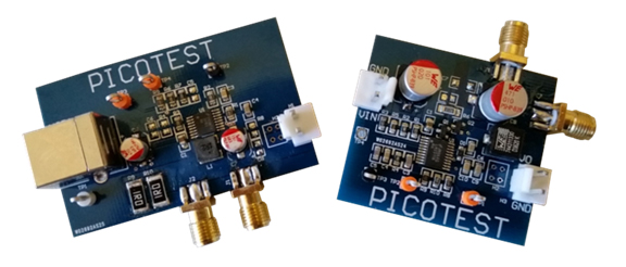
Figure 13 VRM characterization boards include measurement test points for PSRR, output impedance, and error amplifier measurement.
Whether you develop your own test board or use the manufacturer designed evaluation board, access to the error amplifier output is critical to acquiring much of the data needed to support an accurate simulation model.
A parameterized simulation model for Keysight’s ADS simulator software is shown in Figure 14. The model parameters include the sawtooth signal, Vramp, current sense resistor, Ri, and the error amplifier components. These parameters can easily be manually or automatically adjusted to match the PSRR, output impedance, and error amplifier measured data. Additional model elements include the output filter inductance, Lo, output capacitors, switching frequency, Fs, and error amplifier compensation. Alternatively, equations 5, 10 and 13 derived here can be solved simultaneously using any mathematical solver, such as Mathcad’s Minerr.

Figure 14 Parameterized ADS simulation model is tuned to match the measured data.
The parameterized model does not include accurate performance for the current mode resonance shown in Figure 4. In part this is because several adaptations of peak current mode control are in use today and each has a different current loop resonance transformation. The inclusion of any sawtooth ramp minimizes this resonance and restricting the control loop bandwidth to 1/6th of the switching frequency and optimizing the Vramp signal will yield more than acceptable results. Pushing the bandwidth beyond this frequency requires the creation of a much more sophisticated model.
The resulting model allows accurate simulation of AC, time domain, and frequency domain performance, as seen in Figure 15.

Figure 15 A parameterized ADS model supports AC, time domain, and frequency domain simulation. Switching waveforms are achieved using fast harmonic balance simulation. This simulation runs in less than 200ms.
Additional Considerations
In addition to small signal performance, there are other performance criteria worth considering as well as some potential issues to be aware of.
Maximizing efficiency, η, is a major goal for most systems. The most significant power stage losses of the buck synchronous buck converter include the MOSFET conduction losses, output inductor conduction losses, and the freewheel diode losses. In some designs, the freewheel diode is the internal MOSFET body diode and, in other cases, it is an external diode.
The power stage losses can be computed as:

where Rds is the MOSFET on state resistance, Fsw is the switching frequency, Vf is the forward voltage of the body or external freewheel diode, Td is the deadtime, and DCR is the inductor resistance. The impact of dead time and body diode voltage on the efficiency of a buck regulator is shown in Figure 16.
|
Vin=12V |
Iout=10A |
Rdson=2mΩ |
|
Vout=1.2V |
Fsw=2.2MHz |
DCR=1mΩ |

Figure 16 Impact of deadtime on converter efficiency for a typical MOSFET and eGaN FET.
Turn-On and Fault Recovery
Most, but not all VRMs include a soft-start function to prevent overshoot that could exceed the maximum voltage rating of the high-speed devices. Even among those that do include a soft-start function, many do not exhibit soft-start from an overload or short circuit recovery as seen in Figure 17.

Figure 17 Turn on and fault recovery. The VRM on the right lacks soft-start after a fault recovery, resulting in significant overshoot.
Large Signal Response
The small signal response will be the same during large signal events under many conditions. The limitations are related to the dynamic range of the converter, the output filter characteristic impedance, and the slew rate of the error amplifier.
The open loop response of the output can be determined from the transfer of energy between the output inductor, Lo, and the output capacitor, Co. If the inductor current is initially IL and the instantaneous output current change is dIL, then the open loop voltage change is represented in equation 16.

Since IL includes the time varying inductor ripple current, the voltage change is dependent on where in the switching cycle the load change occurs. The voltage transient is, therefore, dependent on where in the switching cycle the load change occurs. In low duty cycle VRMs, the large signal impact is seen on load reduction while in high duty cycle converters the large signal impact is seen on the load increase. Both cases of these responses are shown in Figure 18.

Figure 18 Large signal transient response is related to the dynamic range of the VRM and the characteristic impedance of the output filter.
EMI
The general tendency is to be concerned with the EMI generated at the switching frequency. Much of the EMI, and often the largest EMI signals, are not due to the switching but due to circuit resonances as seen in Figure 19.
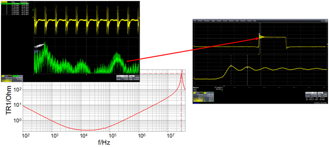
Figure 19 The largest EMI signal is at 30MHz and is due to a PCB plane resonance, seen in the network analyzer impedance plot. The higher frequency is the MOSFET ringing, also PCB related.
The higher frequency EMI signal in Figure 19 is related to the ringing of the MOSFET switch at 160MHz. The EMI from this ringing is related to the ringing time related to the switching frequency. The ringing time is related to the damping or Q of the ring. At higher switching frequency, the same ring time is a larger percentage of the switching cycle and, therefore, contributes more EMI as seen in Figure 20.

Figure 20 The EMI contribution from the ringing is dependent on the time of the ring relative to the switching period.
Conclusions
In this paper, we have defined many of the relationships governing the small signal performance of the buck VRM, as well as the qualitative topological choices and common large signal issues to be aware of. The equations presented allow a model to be developed from a few simple measurements, including PSRR and output impedance.
We have also suggested a proposed improvement to the compensation topology of transconductance feedback amplifiers which greatly improves the performance over the manufacturer’s recommendations.
A recommendation was made to create a simple, easily measured, characterization board for each VRM being considered and to make VRM selections based on the resulting system performance and including tolerance characteristics for the key parameters.
Finally, we have provided insight into the most significant component tolerances, which are not normally specified. Larger companies may be able to obtain the tolerance statistics from the component manufacturers, while smaller companies may need to rely on the measurement of several characterization boards to determine reasonable tolerances.
An earlier version of this paper was a DesignCon 2017 Best Paper Award Winner.
References and Additional Resources
Videos
“How to Design for Power Integrity: Selecting a VRM”, Keysight YouTube, 5/5/2016,
Articles
“Power Integrity: Measuring, Optimizing, and Troubleshooting Power Related Parameters in Electronics Systems”, Steve Sandler, 7/29/2014, McGraw-Hill, ISBN: 0071830995,
“Three stability assessment methods every engineer should know about”, Steve Sandler, 9/8/2016, Signal Integrity Journal.
“Fix Poor Capacitor, Inductor, and DC/DC Converter Impedance Measurements”, Steve Sandler, EEWeb, 10/2016,
“This Misconception About Power Integrity Can Cost You Big”, Steve Sandler, How2Power, 3/2016 http://www.how2power.com/newsletters/1603/H2PToday1603_commentary_Picotest.pdf?NOREDIR=1
“Improve Performance And Reduce Cost”, Steve Sandler, 6/19/2014, Electronic Design,
“How do I pick the best voltage regulator for my circuit?”, Steve Sandler, 9/3/2013, Power Electronics,
“Switch-Mode Power Supply Simulation: Designing with SPICE 3”, Steve Sandler, 11/11/2005, McGraw-Hill, ISBN-10: 0071463267
“Impedance-Based Stability and Transient-Performance Assessment Applying Maximum Peak Criteria” S. Vesti, T. Suntio, J. A. Oliver, R. Prieto, J. A. Cobos, IEEE TRANSACTIONS ON POWER ELECTRONICS Vol 28 Issue 5 2013 pages 2099-2104, 2013
“Optimal Single Resistor Damping of Input Filters”, Robert W. Erickson, 1999 IEEE Applied Power Electronics Conference
Biography
Steve Sandler has been involved with power system engineering for nearly 40 years. Steve is the founder of PICOTEST.com, a company specializing in instruments and accessories for high performance power system and distributed system testing. He frequently lectures and leads workshops internationally on the topics of Power Integrity, PDN, and Distributed Systems and is a Keysight Certified EDA expert.
Steve publishes articles and books related to power supply and PDN performance. His latest book, “Power Integrity: Measuring, Optimizing and Troubleshooting Power-Related Parameters in Electronics Systems” was published by McGraw-Hill in 2014. He is the recipient of the ACE 2015 Jim Williams Contributor of the Year ACE Award for his outstanding and continuing contributions to the engineering industry and knowledge sharing.
Steve is also the founder of AEi Systems, a well-established leader in worst case circuit analysis, modeling, and troubleshooting of satellite and other high reliability systems.