
In high-speed digital channel design, vias are everywhere and are becoming very crucial elements to the channel performance. Especially with the higher data rate requirements in mobile, networking, and data center applications, the effect of vias in a design is very noticeable. Design engineers have traditionally used time domain reflectometry (TDR) as a tool to characterize and optimize via designs, yet the TDR approach comes with shortcomings such as demanding shorter rise-time step signal or larger bandwidth S-parameters, and inaccurate read-out on the via impedance.
In this article, we propose a simple and effective Z-input impedance method that augments the traditional TDR method for characterizing and optimizing via designs in much faster speed systems.
Vias are present in nearly every high-speed digital channel, and they are a crucial part of channel performance. These channels are routed as signal traces on a printed circuit board (PCB) composed of transmission lines and vias, and are the path of signal propagation. Due to the higher data rate requirements, the signal’s wavelength becomes shorter and shorter; therefore, the effect of vias in the design is very noticeable. For example, increased impedance mismatch, higher loss due to the via stub resonances, and potential electro-magnetic interference issues occur. In order to characterize vias in much faster speed systems, we need to have a more efficient and practical way that remedies the shortcomings of the traditional TDR method. The Z input impedance method is a frequency-domain measurement that records via impedance vs. frequency, instead of the time-domain impedance vs distance measurement that a TDR plot would show.
Signal waveforms can be decomposed into a series of Fourier spectral components, and a propagating waveform will experience different impedance values at each of these spectral components. The Z input impedance method will provide the exact impedance value that a propagating waveform will see at each of these spectral components. The Z input impedance method also has no requirement for short risetime step signals or extremely-high-bandwidth S-parameters in order to characterize small via structures. Instead, only measured or simulated S-parameters up to the highest spectral component of interest are needed. Additionally, the parasitics induced by vias, via stubs, non-functional via pads, and functional via pads can be easily related to the frequency dependent Z input impedance profile. This relationship makes it easy for designers to understand, characterize, and optimize the interconnect performance.
TDR to Characterize Vias
TDR has been a great tool for designing high-speed digital channels. It tells the location of discontinuity and relative impedance at that location. For vias, however, TDR has some shortcomings we need to consider. Let us discuss some considerations when using TDR for characterizing vias.
Risetime and Impedance
In order to resolve a very small feature size, such as a via, the rise time of the step signal has to be very short. The minimum feature size (Lmin) that TDR can resolve can be calculated by Eq.1, where TR=risetime(seconds), C0=speed of light(meter/seconds), and εR=relative permittivity. For example, with 10ps rise time, the minimum feature TDR can resolve is approximately 30mils, which is a relatively larger dimension for vias. Any feature size less than 30mils may not be detected at all. Therefore, the minimum resolution must be carefully thought out and a proper selection of step signal with an appropriate rise time for the TDR scopes must be made.

The impedance value shown in Eq 1 is time, or distance, dependent impedance data. Is this impedance constant for all frequencies? Actually, it is not, but it is not obvious from the TDR plot whether the impedance has frequency dependency.
S-Parameter Bandwidth and Impedance Read-out
TDR also can be performed with frequency domain S-parameter data by getting an impulse or step response. Since S-parameters are band-limited frequency data, higher bandwidth frequency data is required to resolve a very small feature size, like vias. Otherwise, small features like vias may not be seen or resolved in the TDR plot, and the impedance read-out value may be incorrect, since the next reflected wave comes back before the previous reflection has settled down.
One example is shown in Figure 1, with a 99.82mil-long through via with via pads at the top and bottom. With 10GHz bandwidth S-parameter, the impedance at the peak is 51.5ohm. But this value increases to 56.5ohm with a 50GHz S-parameter. Now, this higher bandwidth data also starts to reveal the via pads, which are capacitive in nature. This illustrates that the impedance read-out value from the conventional TDR should be used carefully by computing the required bandwidth properly.
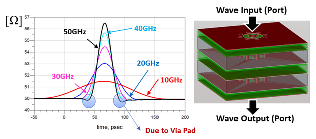
Figure 1.TDR impedance vs. bandwidth for a through via
Z Input Impedance Method
As discussed, TDR comes with its shortcomings; although, it has been a great tool in the last few decades. In this article, we introduce a Z input impedance method to characterize and optimize vias.
With a two-port network, the input impedance is simply described as in Eq 2.

For 50-ohm reference system, Eq.2 becomes Eq.3.

In this article, we propose to use this Z input impedance to characterize and model vias. Since the other port of the two-port network is 50ohm terminated, the magnitude of Z input impedance is centered around 50ohm as shown in Figure 2. (The Z input impedance fluctuates from 46ohm to 67ohms as a function of frequency in this example.) Now, we see that the via impedance is not constant, but varies with the frequency.
Frequency Dependent Via Impedance
Since the via impedance varies over a frequency range, each spectral component of a signal will experience a different impedance for the via. Hence, the reflection or impedance mismatches produced by the via should also vary accordingly. The Z input impedance method allows design engineers to see the frequency dependent impedance characteristic of vias, which helps or augments the traditional TDR method of seeing the impedance along time or distance.
In Figure 2, the Z input impedance increases (or has a positive slope) from DC to 17GHz. It is interpreted as “inductive” since the impedance increases with the frequency. Then it becomes “capacitive” from 17GHz to 34GHz, since the impedance decreases with the frequency. This behavior repeats, and we can easily conclude that the via has both inductive and capacitive characteristics.
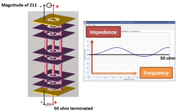
Figure 2. Z input impedance impedance of a via with one end 50ohm terminated
By examining these findings, interestingly, we see that the via impedance profile is very similar to that of a low pass filter’s Z input impedance or ideal transmission-lines as shown in Figure 3.
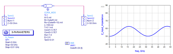
Figure 3. Z input impedance example of an ideal transmission line
No Frequency to Time Conversion Required
Unlike in the TDR case, we see the exact impedance of via at every frequency. There is no frequency to time conversion involved, so designers do not need to worry about the bandwidth of S-parameter nor the rise time for the step signal as in the TDR. Figure 4 shows a comparison of the impedance values between Z input impedance and TDR for the same via structure. This plot allows us to contrast the impedance versus the location or time in TDR compared to the impedance versus frequency in the Z input impedance method.
The TDR impedance at the peak shows 56ohm. The Z input impedance changes from 46ohm to 66ohm. The impedance value from TDR is close to the averaged impedance for a range of frequencies.

Figure 4. TDR impedance vs. Z input impedance
Z input impedance plot with typical via structure
Figure 5 shows various Z input impedance values for varying size of via pads, anti-pads, etc. In general, increasing via pads increases the capacitance, thus pulling the impedance slope down. If we see the inductive slope (positive), we can bring it down by increasing the size of via pads. However, the size of anti-pads is opposite to this behavior: the smaller the size, the larger the capacitance. The existence of non-functional via pads adds capacitance to the impedance, meaning that the impedance slope will come down when introduced.

Figure 5. Various Z input impedance plots
For the ground return vias, two aspects need to be considered. The first is the number of ground vias and the other is the distance from the signal via. More ground vias reduce the inductance for signal via impedance, making the propagation mode close to TEM mode and mimicking a coaxial transmission line. In this condition, the via impedance calculated as a coaxial transmission line is quite close to the real via impedance. However, this only holds with a via structure with a coax style ground via ring design. With a closer ground vias located to the signal via, the impedance slope decreases, since it makes the inductive loop size smaller.
Validation
Next, we validate the Z input impedance method for several test cases with PCB measurements. Since there are many variables such as via pads, anti-pads, via barrel, and non-functional via pads, for simplicity, this analysis uses a fixed size for via pads, via barrel, and ground via to anti-pad distance: 26mil diameter, 12mil diameter, and 3mil respectively.
PCB Stackup
The stackup has a very large impact on the performance of a PCB. If high frequencies are present in the system, then careful consideration should be given to the material types and thickness of both conductors and insulators on each layer of the stackup. We used a common copper clad glass weave/epoxy structure to build up the test PCB stackups. The dielectric was Isola FR408HR. It has a lower loss tangent (0.0085~0.011) and dielectric constant (3.24~3.99) in comparison with many other common FR-4 variants, meaning it will exhibit less loss on high frequency signals. In some cases, more exotic materials may be required if a glass weave does not meet the necessary electrical characteristics of a system, but by using lower cost materials in our tests the results may correlate with a great number of other designs. The over-all thickness of the board also limits the size of vias that can be used. This is referred to as via aspect-ratio, which is a measurement of via length (stackup thickness) divided by via drill diameter.
Manufacturing Tolerences
When it comes to validating simulation data, it is critical to make a distinction between an ideal layout designed in CAD software, and an actual PCB fabricated to the CAD specifications. There is no perfect manufacturing process, and tolerances must be kept in mind on all structures, for example, material thickness, non-homogenous materials, via drill wander, and plating inconsistencies. Some examples are shown in Figure 6.

Figure 6. Examples of manufacturing tolerances
The other consideration is the variation of the material properties such as the dielectric constant, which changes the electrical length of via. The Dk/Df also vary with frequency, which will affect the simulation accuracy as well.
Measurements
Via measurements are often challenging due to their small electrical length when compared to the test hardware, cables, probes, connectors, etc. If the measurement setup and calibration are not optimal, their imperfections will show up in the test results. In addition, vias often tend to resonate if the signal is not launched in a symmetrical manner. In this article, we used coaxial and probes measurement techniques, each of which has their strengths and weaknesses. So, the idea is for the two techniques to complement each other to achieve the best results possible. Connectors are ideal for larger structures whose propagation mode is TEM, while probes work best for smaller structures which can support point-source launches without too many secondary effects shown in Figure 7.
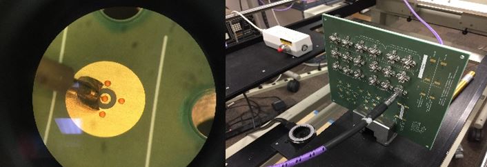
Figure 7. Probe vs. Coaxial measurement
In either case, the calibration needs to be verified to ensure the best accuracy possible. The ideal standard for coaxial calibration is a measurement-grade adapter to which both cables can be connected and the insertion-loss verified. For probes a coplanar line serves the same purpose. This data needs to be saved each time the system is calibrated so deviations in the measurements can be objectively quantified
Validation Results
In this section, we compare the simulation data to measured data for two structures. We used ADS (Advanced Design System) and EMPro (Electro-Magnetic Professional) for the simulations:
- 2.92mm connector <--> Through Via with 4 return path vias <--> 2.92mm connector, NFVP removed
- 2.92mm connector <--> Through Via with 2 return path vias <--> 2.92mm connector, NFVP removed
These structures give us a sense of how the number of return path vias affects via-structure impedance.

Figure 8. The via structure sandwiched by two 2.92mm connectors
4 ground vias:
In Figure 9, the Z input impedance fluctuates from 30ohm to 75ohm. At lower frequencies, the Z input impedance starts as slightly inductive but maintained less than 55ohm. The TDR peak impedance at the middle of via is close to 60ohm from the TDR plot.

Figure 9. Z input impedance and TDR for 4 ground via case
The Z input impedance plot shows the noise on the impedance data around 25GHz, which is due to the cavity or plane modes generated in PCB. However, this is not seen, and it is not obvious whether these modes exist in the TDR plot. The comparison between the two plots shows how much more informative the Z input impedance method is when characterizing a via.
2 ground vias:
In Figure 10, the impedance slope gets steeper, meaning that the via impedance characteristic becomes more inductive compared to Figure 9.

Figure 10. Z input impedance and TDR for 2 ground via case
By comparing the results of Z input impedance from Figure 9 and Figure 10, it can be seen that Z input impedance becomes more inductive when the number of return-path vias is decreased. The agreement between simulated and measured data looks very good, even picking up unwanted modes in Figures 9 and 10. The electric field plots at 10GHz and 21GHz for the Figure 10 case are shown in Figure 11. The electric field strength (V/m) is plotted with different colors, red for strongest and blue for weakest. At 10GHz, the electric field is confined well within the vincinity of via, similar to TEM mode of propagation. However, at 21GHz, the unwanted modes are clearly seen as picked up by the Z-input impedance plot.

Figure 11. Electric field plots at vertical and horizontal cross-section at 10GHz and 21GHz
Conclusion
In this article, we proposed a Z input impedance method that augments or overcomes some shortcomings of the traditional TDR method. The purpose of this work is to introduce this concept of a Z input impedance method for modeling via structures. This technique helps design engineers understand the frequency dependent impedance characteristic of vias without having difficulties related to the rise-time of step signal or band-limited S-parameters. By combining Z input impedance with traditional TDR methods, design engineers can gain more insight for via designs and will be able to optimize vias for better channel performance.
There are many opportunities to expand upon this work. Our interest is focused on single-ended structures with a high return-path via count. In high-speed interfaces, differential signaling and differential via structures are much more commonly used.
These differential structures should be examined in a similar process to characterize their impedance profiles and how via anatomy modifications can affect over-all impedance. Additionally, it is also more common in PCB design to use 1 or 2 return path vias instead of 8. This more common structure should be explored further and characterized so that impedance can be modeled and controlled.
References
- High-Speed Digital Design, Howard Johnson, Prentice Hall 1933 ISBN-13: 978- 0133957242, ISBN-10: 0133957241
- Signal and Power Integrity Simplified, Eric Bogatin, Prentice Hall 2009 ISBN-13: 978-0132349796, ISBN-10: 9780132349796
- Modeling On-Board Via Stubs and Traces in High-Speed Channels for Achieving High Data Bandwidth, Ki Jin Han et. el, IEEE Transaction on Components, Packaging and Manufacturing Technology, Vol.4, No.2, February 2014
- Effects of open stubs associated with plated through-hole vias in backpanel designs, Chen Wang, et el. EMC 2004 International Symposium
- Practical Analysis of Backplane Vias, Eric Bogatin, Bert Simonovich, Sanjeev Gupta, Mike Resso, DesignCon 2009, Santa Clara, CA
- Signal Integrity Characterization Techniques, Mike Resso & Eric Bogatin , IEC
- State of the Art in EM Software for Microwave Engineers, White Article, 5990-3225EN, Jan Van Hese, Hee-Soo LEE