Technical Articles
Outer Loop Equalization for PCIe Cross-Lane Transceiver Optimization
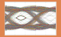
PCIe Gen4 Standards Margin-Assisted Outer-Layer Equalization for Cross-Lane Optimization in a 16GT/s PCIe Link
Read More
Managing EMI and EMC at GHz and Beyond
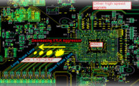
Tools to Combat Radiated Emissions, for EMC Compliance and Performance Gains
Read More


