
With PCIe Gen7 on the horizon, expected to debut around 2025 at a staggering 128 GT/s data rate and a pad-to-pad channel loss budget shift from 32 dB @ 16 GHz to 36 dB at 32 GHz, this paper delves into the evolving performance requirements for Gen7 connectors and details the pivotal design changes needed to meet these demands.
The study delves into meticulous design refinements in both the add-in card and baseboard components, addressing challenges such as signal integrity concerns, ground-mode resonances, and the delicate balance between signal performance and mechanical reliability. From adjustments in edge-finger dimensions to the strategic placement of ground vias, these enhancements demonstrate a commitment to meeting stringent specifications accompanying the bandwidth increase.
Additionally, the paper presents a thorough analysis, encompassing impedance, Return Loss, and Insertion Loss comparisons between the PCIe Gen6 and Gen7 connector. These analyses emphasize the indispensable role of rigorous impedance control and meticulous connector design in effectively navigating the escalating data rates. Thoughtful consideration of simulation parameters, including frequency and solver type, ensures precise modeling, providing an in-depth understanding of the connector's impedance characteristics.
Introduction
As the data rate of PCIe Gen7 soars to an impressive per lane transfer rate of 128 Gbps using PAM-4 modulation, mirroring the advancements seen in the Gen6 standard, the market will undoubtedly witness an increased demand for a cutting-edge Card Electromechanical (CEM) connector. This connector must not only seamlessly operate at the elevated data rate but also maintain mechanical backward compatibility, addressing the evolving needs of customers.
The successful realization of this ambitious goal for PCIe Gen7 heralds a new era, where the Gen7 specification would boast a remarkable fourfold increase in bandwidth compared to its Gen5 counterpart. This leap in performance signifies a substantial advancement in data transfer capabilities, promising to revolutionize the landscape of connectivity and pave the way for more efficient and powerful computing systems.
The CEM connector faces a pivotal moment demanding significant internal design adaptations to accommodate this expansive frequency range. Striking a delicate balance between technological advancement and backward compatibility, the outside envelope dimensions of the CEM connector must remain unaltered to seamlessly integrate with previous PCIe generations.
In maintaining the essential features of the Gen6 Add-in Card (AIC), including the core shielding ground plane, fingertip south vias, and lateral ground bar, we have introduced a notable enhancement. This involves the incorporation of blind vias that establish connections from the topmost layer to the innermost ground layer.
Furthermore, a meticulous adjustment in the baseboard design became imperative. To mitigate resonances and elevate the insertion loss (IL) drop-off frequency to a higher range, supplementary GND vias have been strategically inserted at the center of the ground pad. These modifications are detailed in the subsequent section, providing a comprehensive understanding of the refined AIC and baseboard designs.
The interface between the AIC and the connector plays a pivotal role in shaping the Signal Integrity (SI) performance of the connector as a whole. Elevating the impedance match within this crucial mating area directly enhances not only the Return Loss (RL) but also the Insertion Loss and Insertion Loss Deviation for the entire channel. This becomes particularly paramount at higher data rates, where stringent considerations are imperative.
Given the accelerated pace of data transmission, minimizing impedance mismatches in the mating area becomes instrumental in preserving the integrity of the signal. The significance lies in preventing substantial portions of the channel loss budget from being absorbed by large impedance disparities, safeguarding the efficiency and reliability of the entire communication channel. In essence, optimizing the mating area becomes a linchpin for ensuring robust SI performance in the face of escalating data rates. This required a reduction in the signal pad length on the AIC to 2.0 mm, marking a 0.5 mm reduction from the south side of the Gen6 pad length, previously measured at 2.5 mm.
Figure 1 illustrates the architecture of the PCIe CEM connector. When we talk about connector only performance of CEM connector, it encompasses approximately 50 mils of trace on the AIC, the pad on the AIC where the connector mates, the connector itself, the pad on the baseboard where the connector is affixed, and an additional 50 mils of trace on the baseboard.
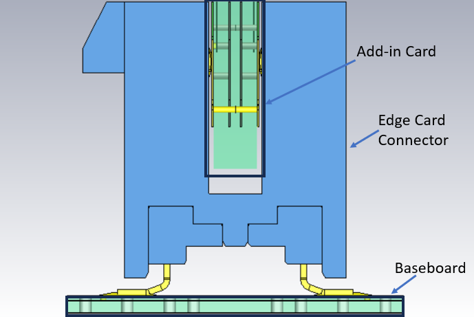 Figure 1. Architecture of the PCIe CEM connector.
Figure 2 shows the simulated impedance comparison of PCIe Gen6 CEM connector against the PCIe Gen7 CEM connector. For optimal Signal Integrity (SI) performance in Card Electromechanical (CEM) connectors, a general guideline suggests maintaining impedance within ±10% of 85 Ω . However, the Gen6 connector demonstrates significant impedance mismatches during the faster 10ps rise time, with maximum and minimum impedances reaching 96 Ω and 72 Ω , respectively. These deviations significantly impact performance, as evidenced in the IL and RL comparisons illustrated in Figure 3 and Figure 4. Notably, after 8 GHz, the IL and RL for the Gen6 connector diverge and exceed the acceptable limits set by the frequency masks at 22 GHz. These frequency masks for IL and RL are essentially extensions of the Gen6 standards, adjusted to accommodate the higher Nyquist frequency of the Gen7 connector. These results show that the need for stringent impedance control becomes more critical as data rates rise.
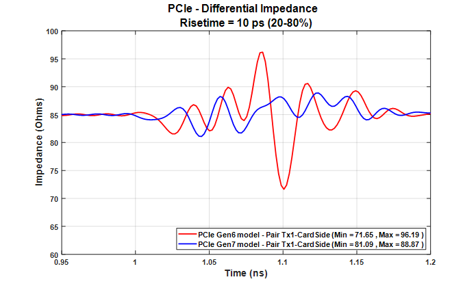 Figure 2. Impedance comparison of Amphenol’s PCIe Gen6 connector vs. Gen7 connector.
 Figure 3. Return loss comparison of Amphenol’s PCIe Gen6 connector vs. Gen7 connector.
 Figure 4. Insertion loss comparison of Amphenol’s PCIe Gen6 connector vs. Gen7 connector.
 The performance of Gen6 and Gen7 connectors, when integrated into a channel, has also been evaluated using the Seasim software. Specifically, the analysis focused on how these connectors operate within a Gen6 channel, employing standard Gen6 reference packages provided by the Seasim software. The findings, depicted in Figure 5, reveal that at a bit error rate (BER) of 1e-06, the top eye height (EH) and top eye width (EW) metrics for the connectors exhibit noticeable differences. For the Gen6 connector, the top eye height is 41.54mV, and the top eye width is 0.180 unit intervals (UI). In contrast, the Gen7 connector shows an enhanced performance with a top eye height of 43.17mV and a top eye width of 0.205 UI.
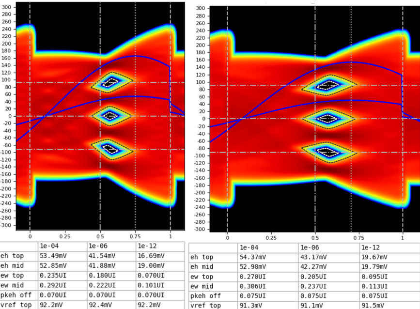 Figure 5. Seasim results comparing Gen6 (left) and Gen7 (right).
In the pursuit of optimal connector design, impedance matching and minimizing unnecessary Insertion Loss are crucial considerations. However, designers face an additional challenge in steering clear of resonances. The PCIe Gen7 connector, like any connector with multiple ground conductors or return paths for current, is susceptible to ground-mode resonances—a challenge notorious for its complexity in elimination.
The presence of multiple grounds introduces the potential for different voltages, giving rise to unexpected propagating modes. These modes often manifest as subtle, narrow dips in Insertion Loss and sharp spikes in crosstalk.
Add-in Card Design
Within the Gen7 AIC, the top edge of the edge-finger resides 5.1 mm above the bottom edge of the AIC, incorporating a nominal wipe of 1.1-1.3 mm. As we venture into higher frequency ranges, the inevitable reduction in wipe length becomes a strategic necessity to address signal integrity concerns. However, this poses a challenge for mechanical integrity, requiring engineers to grapple with devising robust clamp mechanisms. These mechanisms play a pivotal role in ensuring the stability of the AIC within the connector, underscoring the intricate balance between signal performance and mechanical reliability in the pursuit of optimal Gen7 design.
Inner ground plane layers are located at a depth of 20.5 mils beneath the edge finger region in PCIe Gen7 AIC to improve the NEXT and to reduce the impact on other parameters such as parasitic coupling to the edge fingers. Another feature in Gen7 AIC is South GND via and lateral ground bar connecting all the south GND via. The amalgamation of these features with the inner ground planes has demonstrated a marked reduction in NEXT, which prompted their inclusion in the Gen5 AIC design.
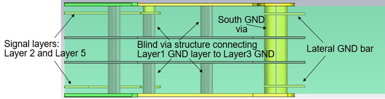 Figure 6. AIC design of PCIe Gen7 CEM connector.
The enhancement introduced in the Gen7 AIC, compared to its Gen6 predecessor, is the integration of blind vias. These vias create direct ground connections from the top layer to the innermost ground layer. Figure 7 shows the degradation in IL performance after 25 GHz with the removal of these blind vias.
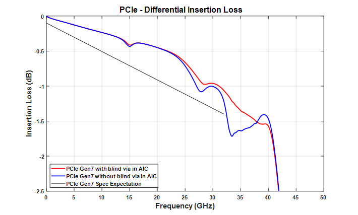
Figure 7. Insertion loss performance with and without blind via in AIC.
Baseboard Design
Illustrated in Figure 8 is the baseboard/motherboard footprint, featuring ground vias positioned at both ends of the ground pads. The purpose of adding ground via on both sides is to reduce the overall inductance in the ground, (i.e. return path), and this mitigates some of the ground-mode resonances.
In addition to the mitigation of the resonances, the FEXT experiences an overall improvement in its baseline level. Poor or compromised ground structures can permit so called ground bounce noise which can cause or exacerbate FEXT. The additional ground vias provide additional paths which tie together the ground planes and improves the overall integrity of the ground reference thus reducing FEXT.
The Gen7 version retains the Gen6's baseboard footprint; however, to accommodate higher frequency operations, modifications to the baseboard are necessary. A key adjustment involves adding an extra GND via at the center of the GND pad to enhance performance at higher frequencies.
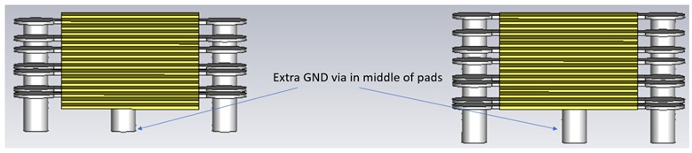 Figure 8. Addition of extra GND via in baseboard.
Figure 9 illustrates a decline in IL performance beyond 25 GHz, alongside a pronounced resonance peak at 32 GHz, attributable to the elimination of additional GND vias in the center of the GND pad.
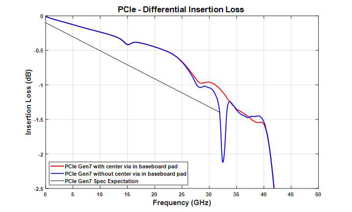 Figure 9. Insertion loss performance with and without center GND via in baseboard.
Simulation Parameters
As data rates continue to rise, the simulation frequency required to solve the model also increases. A higher simulation frequency corresponds to greater spatial resolution in Time Domain Reflectometry (TDR) results. The impedance plots presented below illustrate TDR outcomes derived from S-parameter models, generated through simulations in CST and HFSS, each solved up to 50 GHz and 128 GHz, respectively.
Examining the impedance plots at these elevated frequencies reveals a notable difference in impedance within the 1.02-1.03 ns range. Therefore, in correlating simulation results with actual measurements, utilizing models that extend to higher frequencies yields more accurate correlations and aids in design troubleshooting. However, this approach requires a trade-off in the form of extended simulation durations. It is crucial to recognize that CST results were obtained using a time domain solver, while HFSS results employed a frequency domain solver. This observation underscores the significance of considering both the simulation frequency and solver type in analyzing the impedance characteristics of the model.
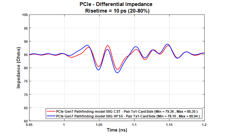 Figure 10. Impedance plot comparing CST and HFSS results solved to 50 GHz.
 Figure 11. Impedance plot comparing CST and HFSS results solved to 128 GHz.
Figure 11. Impedance plot comparing CST and HFSS results solved to 128 GHz.Connector Housing Material
Another critical factor that affects the insertion loss performance of the connector is the Dissipation factor (Df) value of the housing material utilized. In the plot below, it compares the insertion loss performance of the connector with Df values of 0.02 and 0.006. Employing a housing material with a lower Df value gave a significant boost to push the insertion loss drop off frequency further by about 1-2 GHz and giving more margin with respect to the spec line.
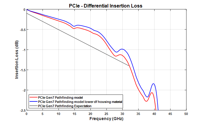 Figure 12. Insertion loss improvement with use of lower Df material for housing of connector.
Conclusion
In conclusion, the evolution from PCIe Gen6 to Gen7 marks a significant milestone in the realm of high-speed data transfer, with the Gen7 standard achieving an unprecedented 128 Gbps per lane transfer rate through PAM-4 modulation. The demand for a state-of-the-art CEM connector, seamlessly compatible with this elevated data rate while preserving mechanical backward compatibility, has never been more critical. The meticulous enhancements detailed throughout this paper, from the integration of blind vias to the strategic addition of GND vias, underscore a dedicated effort to refine both the AIC and baseboard designs to meet the rigorous demands of the Gen7 specification. The impedance, RL, and IL comparisons between PCIe Gen6 and Gen7 connectors reveal the paramount importance of strict impedance control and the necessity for an impeccably designed connector to satisfy the heightened performance criteria. The decision to maintain the Gen6 baseboard footprint while introducing critical modifications illustrates a commitment to backward compatibility without compromising on performance enhancements necessary for Gen7's success. The precision in simulation parameters, including frequency and solver type considerations, ensures an accurate modeling approach, fostering a deep understanding of the connector's impedance characteristics.
Key numerical findings from the analysis include:
- The Gen7 connector demonstrate a top eye height of 43.17mV and a top eye width of 0.205 UI, in contrast to the Gen6 connector which show a top eye height of 41.54mV and a top eye width of 0.180 UI in a Gen6 channel.
- Significant impedance mismatches were observed with the Gen6 connector during faster 10 ps rise times, reaching maximum and minimum impedances of 96 Ω and 72 Ω, respectively, which significantly impacted performance beyond 8 GHz.
REFERENCES
- S. Smith and M. Rengarajan, "Overcoming the SI Challenges in Designing 25-40 Gb/s Backplane Channels," DesignCon 2014.
- Y. Li and Y. Huang, "PCIe Gen5 CEM Connector and Add-in Card PCB Design Optimizations," DesignCon 2019.
- PCI Express CEM Specification, Rev. 5.0 Version 1.0.
- PCI Express CEM Specification, Rev. 6.0 Version 0.5.
- PCIe Revision 7.0 Version 0.5 Electrical Specification.